Cross talk and interference reduction for high frequency wireless interconnects

a high-frequency wireless and interconnect technology, applied in the direction of antennas, antenna details, antenna couplings, etc., can solve the problems of affecting the mechanical and thermal assembly requirements of the assembly, requiring additional complexity in the design of the socket, and increasing the input/output (i/o) density,

Active Publication Date: 2018-07-26
INTEL CORP
View PDF3 Cites 3 Cited by
  • Summary
  • Abstract
  • Description
  • Claims
  • Application Information

AI Technical Summary

Problems solved by technology

However, with increasing data rates, the Input/Output (I/O) density increases and requires additional complexity in the design of the socket that conne

Method used


Image

  • Cross talk and interference reduction for high frequency wireless interconnects
  • Cross talk and interference reduction for high frequency wireless interconnects
  • Cross talk and interference reduction for high frequency wireless interconnects

Examples


Embodiment Construction

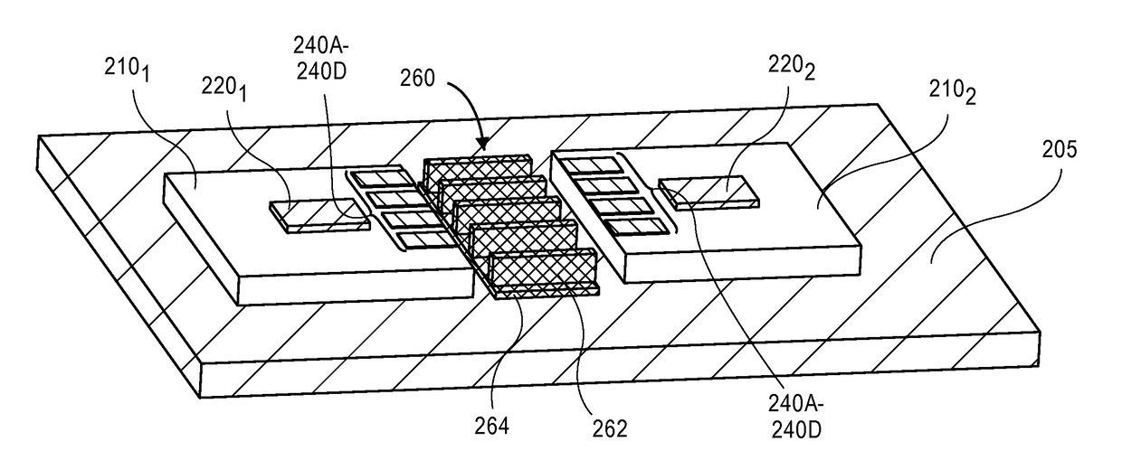
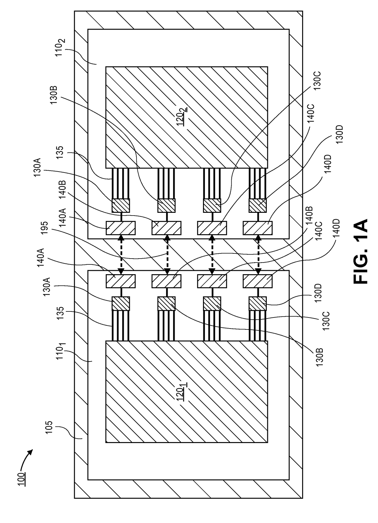
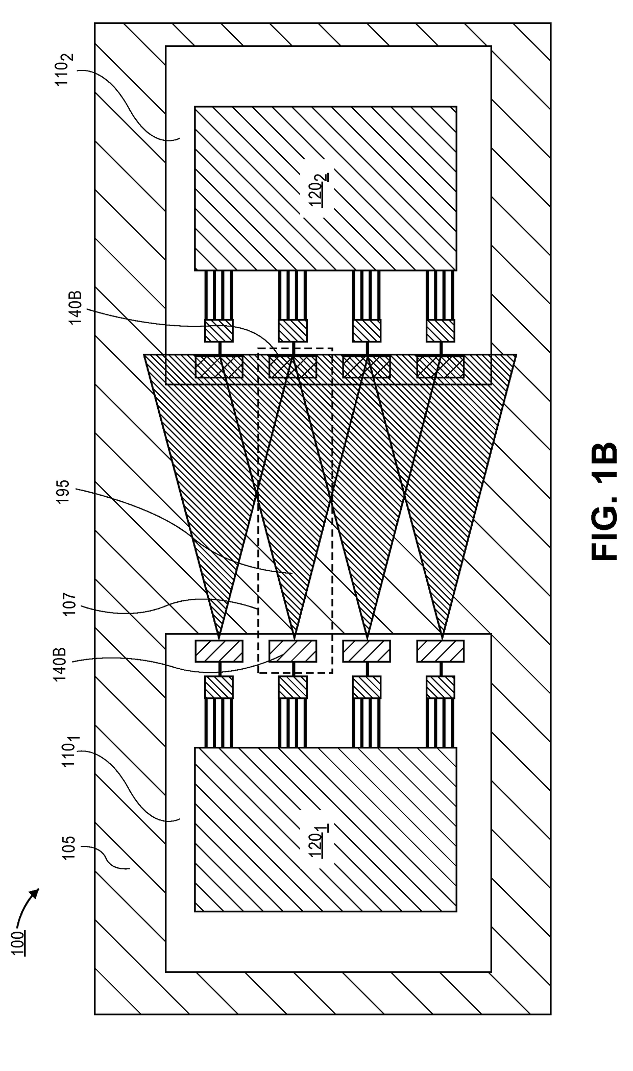
[0017]Described herein are systems that include a device package with wireless interconnects that have reduced cross-talk and interference between the wireless interconnects. In the following description, various aspects of the illustrative implementations will be described using terms commonly employed by those skilled in the art to convey the substance of their work to others skilled in the art. However, it will be apparent to those skilled in the art that the present invention may be practiced with only some of the described aspects. For purposes of explanation, specific numbers, materials and configurations are set forth in order to provide a thorough understanding of the illustrative implementations. However, it will be apparent to one skilled in the art that the present invention may be practiced without the specific details. In other instances, well-known features are omitted or simplified in order not to obscure the illustrative implementations.

[0018]Various operations will ...


PUM


Abstract

Embodiments of the invention may include packaged device that may be used for reducing cross-talk between neighboring antennas. In an embodiment the packaged device may comprise a first package substrate that is mounted to a printed circuit board (PCB). A plurality of first antennas may also be formed on the first package. Embodiments may also include a second package substrate that is mounted to the PCB, and the second package substrate may include a second plurality of antennas. According to an embodiment, the cross-talk between the first and second plurality of antennas is reduced by forming a guiding structure between the first and second packages. In an embodiment the guiding structure comprises a plurality of fins that define a plurality of pathways between the first antennas and the second antennas.

Description

FIELD OF THE INVENTION[0001]Embodiments of the present invention relate generally to the manufacture of semiconductor devices. In particular, embodiments of the present invention relate to wireless interconnects in semiconductor packages and methods for manufacturing such devices.BACKGROUND OF THE INVENTION[0002]In many computer systems multiple integrated circuit chips communicate with each other to perform the programmed operations. The different chips may include central processing units, high speed memories, mass storage devices, chipsets, video processors, and input / output interfaces. Some computers may have more than one of each of these kinds of chips. The chips are traditionally mounted to a motherboard or system board either directly or through a socket or a daughter card.[0003]The chips traditionally communicate using copper interconnects or links that travel through the chip's package vias, through the socket, through the platform motherboard and then back through the soc...

Claims


Application Information

Patent Timeline
IPC IPC(8): H01Q1/52H01Q1/22
CPCH01Q1/521H01Q1/2283H01Q1/38H01Q1/2266H01Q1/525H01Q21/28
Inventor ELSHERBINI, ADEL A.KAMGAING, TELESPHOROSTER, SASHA N.DOGIAMIS, GEORGIOS C.
Owner INTEL CORP
Why Eureka
Try Eureka