Inter-chip wireless interconnection structure

An interconnection structure and chip-to-chip technology, applied to electrical components, electrical solid devices, circuits, etc., can solve problems such as signal crosstalk, signal delay attenuation, and increase in the number of circuit board layers, so as to avoid interference, ensure communication, and eliminate metal The effect of wire connection method

Inactive Publication Date: 2016-04-20
NANJING UNIV OF AERONAUTICS & ASTRONAUTICS
View PDF3 Cites 3 Cited by
  • Summary
  • Abstract
  • Description
  • Claims
  • Application Information

AI Technical Summary

Problems solved by technology

On the one hand, the dense wires cause crosstalk between signals; on the other hand, there will be many through holes on the printe

Method used


Image

  • Inter-chip wireless interconnection structure
  • Inter-chip wireless interconnection structure
  • Inter-chip wireless interconnection structure

Examples


Embodiment Construction

[0025] Embodiments of the present invention are described in detail below, examples of which are shown in the drawings, wherein the same or similar reference numerals denote the same or similar elements or elements having the same or similar functions throughout. The embodiments described below by referring to the figures are exemplary only for explaining the present invention and should not be construed as limiting the present invention.

[0026] The inter-chip wireless interconnection structure of the present invention combines the respective physical structures and spaces of chips and printed circuit boards, and exerts their functions that have not been used before.

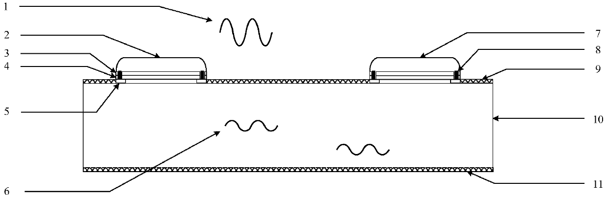
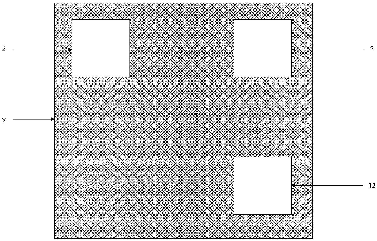
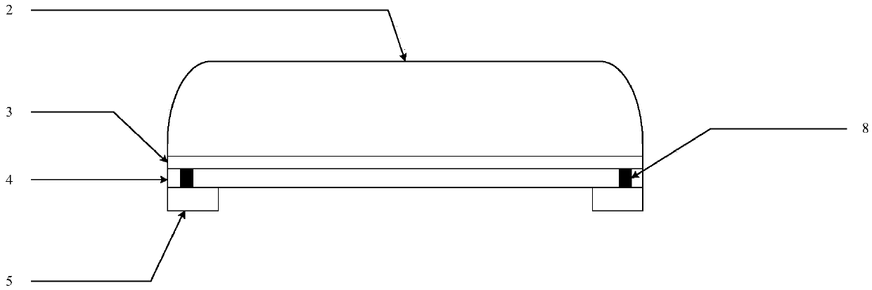
[0027] like figure 1 As shown, the inter-chip wireless interconnection structure of the present invention includes a patch pin antenna with a chip, a printed circuit board medium and a wave-absorbing layer. The patch pin antenna of the chip is made up of metal heat sink 3, chip package bottom 4, through hole ...


PUM


Abstract

The invention discloses an inter-chip wireless interconnection structure. According to the structure, SMD pins of chips are taken as transmitting antennae and receiving antennae, and electromagnetic waves are transmitted in a circuit board medium; furthermore, the upper surface of a circuit dielectric slab is coated with a layer of wave-absorbing material, and the lower surface of the circuit dielectric slab is coated with a layer of wave-absorbing material, so that communication between chips and communication between chips and the outside are isolated and electromagnetic interference is reduced. The SMD pins of chips and the circuit board medium are utilized, the physical structure and unused space of the circuit board are fully used, circuit integration is further achieved, and the size is reduced.

Description

technical field [0001] The invention relates to a wireless interconnection structure between chips, in particular to a wireless interconnection structure for communication between two or more chips, and belongs to the technical field of inter-chip wireless communication. Background technique [0002] Today's electronic products are becoming more and more intelligent, and the commands that need to be processed by the chip are also increasing, and the peripheral circuits connected to the chip are also inevitably increasing. The connection between the chip and the peripheral circuit uses metal copper wires, and there will be different degrees of crossing or paralleling between these wires. On the one hand, the dense wires cause crosstalk between signals; on the other hand, there will be many through holes on the printed circuit board, which introduces signal delay, attenuation, etc.; finally, the number of layers of the circuit board will increase. [0003] At present, some so...

Claims


Application Information

Patent Timeline
IPC IPC(8): H01L23/52H01L23/367
CPCH01L23/52H01L23/367
Inventor 王文松曹群生王毅
Owner NANJING UNIV OF AERONAUTICS & ASTRONAUTICS
Why Eureka
Try Eureka