Display and compensation circuit therefor

a compensation circuit and display technology, applied in the field of display and compensation circuit therefor, can solve the problems of reducing the aperture ratio of the conventional amoled display, severely attenuating the supply voltage, and reducing the uniformity of light emitted

Active Publication Date: 2011-08-25
NAT CHENG KUNG UNIV
View PDF2 Cites 70 Cited by
  • Summary
  • Abstract
  • Description
  • Claims
  • Application Information

AI Technical Summary

Benefits of technology

[0014]According to one more aspect of the present invention, a display comprises a plurality of scan lines, a plurality of data lines, a plurality of pixel circuits, a compensation circuit, a voltage controller, and a data line driver. The data lines form junctions with each of the scan lines. Each of the pixel circuits is disposed at a corresponding one of the junctions of the scan lines and the data lines, and includes a light-emitting member. When one of the scan lines and one of the data lines are driven, one of the pixel circuits on the junctions of said one of the scan lines and said one of the data lines is activated, and generates a driving current that drives the light-emitting member thereof to emit light. The compensation circuit is coupled to the pixel circuits, and is operable so as to generate a voltage parameter based on the driving current generated by an activated one of the pixel circuits. The voltage controller is coupled to the compensation circuit, and is operable so as to generate a reference voltage that corresponds to a position of the activated one of the pixel circuits with reference to the voltage parameter generated by the compensation circuit. The data line driver is coupled to the data lines and the voltage controller, is adapted to receive an image signal, and is operable so as to correct the image signal received thereby based on the reference voltage generated by the voltage controller, and so as to drive the data lines with the image signal corrected thereby. The compensation circuit includes a plurality of judging devices corresponding in number to the data lines. Each of the judging devices includes a current comparing unit and a lookup table. The current comparing unit is coupled to a corresp

Problems solved by technology

The aforementioned conventional AMOLED display is disadvantageous in that, since the threshold voltage of the second transistor 922 differs from one pixel circuit 9 to another due to manufacturing drift and operating conditions, the driving current generated by the second transistor 922 also differs from one pixel circuit 9 to another.
This, however, reduces an aperture ratio of the conventional AMOLED display.
Moreover, since the length of a l

Method used


Image

  • Display and compensation circuit therefor
  • Display and compensation circuit therefor
  • Display and compensation circuit therefor

Examples


Embodiment Construction

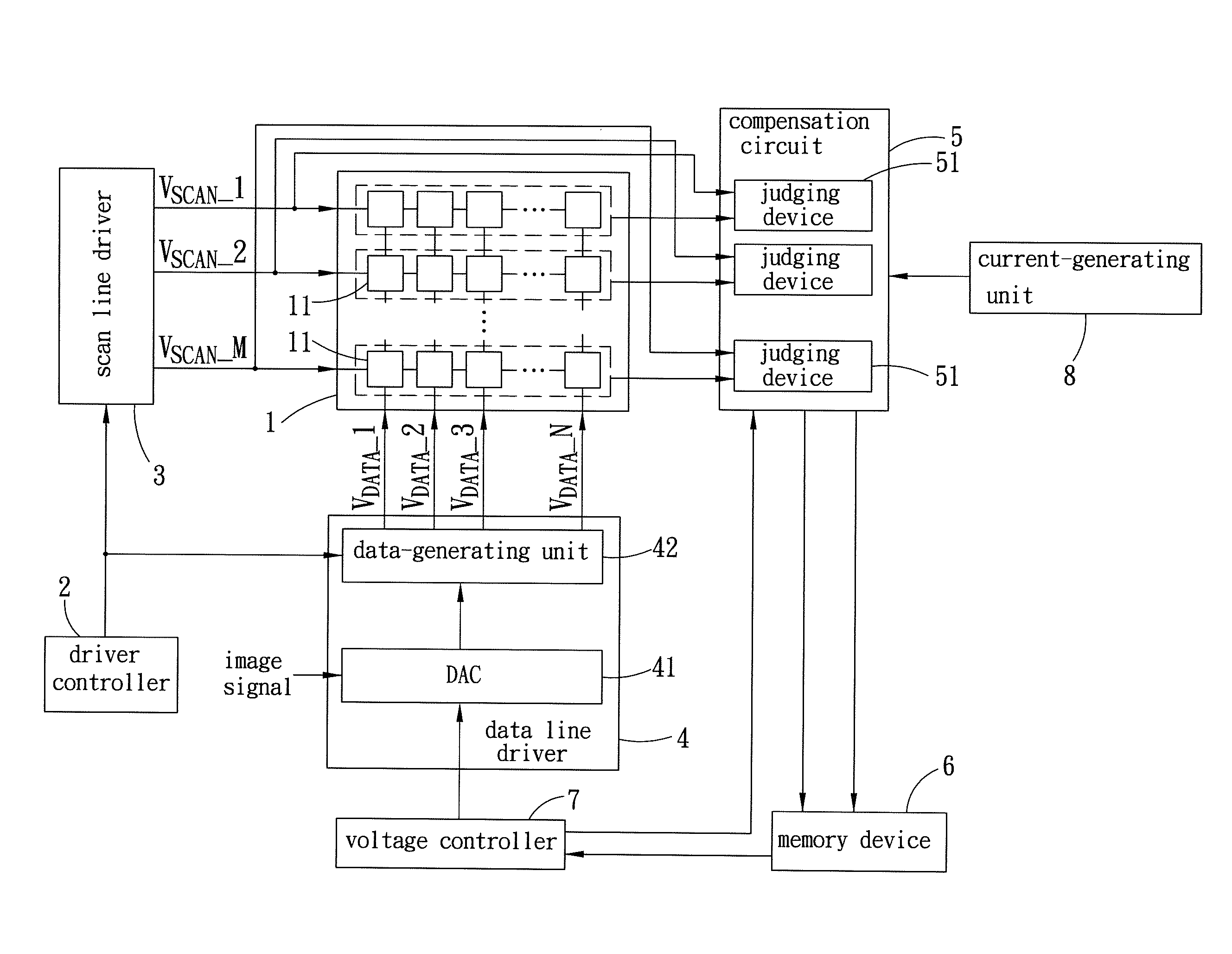
[0033]Referring to FIG. 3, the first preferred embodiment of a display according to this invention is shown to include an array module 1, a compensation circuit 5, a memory device 6, a voltage controller 7, a data line driver 4, and a scan line driver 3.

[0034]The array module 1 includes a plurality of scan lines (VSCAN—1 to VSCAN—M), a plurality of data lines (VDATA—1 to VDATA—N), and a plurality of pixel circuits 11.

[0035]The data lines (VDATA—1 to VDATA—N) form junctions with each of the scan lines (VSCAN—1 to VSCAN—M).

[0036]Each of the pixel circuits 11 is disposed at a corresponding one of the junctions of the scan lines (VSCAN—1 to VSCAN—M) and the data lines (VDATA—1 to VDATA—N).

[0037]With further reference to FIG. 4, each of the pixel circuits 11 includes a driving member 110, and an organic light-emitting diode (OLED) 120 connected to the driving member 110 thereof.

[0038]The compensation circuit 5 is connected to the array module 1. The memory device 6 is connected to the co...


PUM


Abstract

A display includes a scan line, a data line, a pixel circuit, a compensation circuit, a voltage controller, and a data line driver. The data line forms a junction with the scan line. The pixel circuit is disposed at the junction of the scan line and the data line. When the scan line and the data line are driven, the pixel circuit generates a driving current. The compensation circuit generates a comparing signal and a positioning signal based on the driving current. The voltage controller generates a reference voltage that corresponds to the positioning signal with reference to the comparing signal. The data line driver corrects an image signal based on the reference voltage, and drives the data line with the corrected image signal. A compensation circuit for the display is also disclosed.

Description

BACKGROUND OF THE INVENTION[0001]1. Field of the Invention[0002]This invention relates to a display, and a compensation circuit therefor.[0003]2. Description of the Related Art[0004]FIG. 1 illustrates a conventional active matrix organic light-emitting diode (AMOLED) display that includes a display panel 95, a scan line driver 96, and a data line driver 97. The display panel 95 includes an array of pixel circuits 9. The pixel circuits 9 in each row are connected to a scan line 93, whereas the pixel circuits 9 in each column are connected to a data line 94. The scan line driver 96 is connected to the scan lines 93. The data line driver 97 is connected to the data lines 94. Each of the pixel circuits 9, as illustrated in FIG. 2, includes an OLED 91 and a driving member 92. The driving member 92 has a 2T1C structure, and includes first and second transistors 921, 922 and a capacitor 923.[0005]When one of the scan lines 93 is driven by a scan voltage (VSCAN) generated by the scan line d...

Claims


Application Information

Patent Timeline
IPC IPC(8): G06F3/038
CPCG09G3/2092G09G2320/045G09G2320/043G09G3/3225
Inventor LIN, CHIH-LUNGCHOU, KUAN-WENTU, CHUN-DA
Owner NAT CHENG KUNG UNIV
Why Eureka
Try Eureka