

Test device for display panel and method of testing the same
a test device and display panel technology, applied in the field of test devices for display panels and test methods for display panels, can solve the problems of difficult manufacturing of large-scale or high-precision panels, relatively expensive manufacture of amoled displays, and difficult to implement amoled display control methods, etc., to achieve removal or prevention of stain defects of screens, high image quality, and reduced power consumption
- Summary
- Abstract
- Description
- Claims
- Application Information
AI Technical Summary
Benefits of technology
Problems solved by technology
Method used
Image

Examples
Embodiment Construction
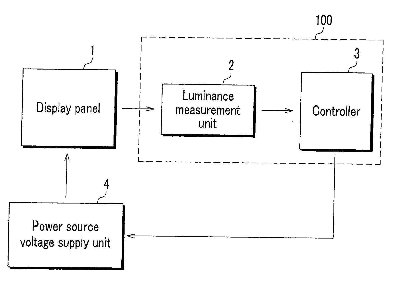
[0048]Certain exemplary embodiments according to the present invention will be described more fully hereinafter with reference to the accompanying drawings. As those skilled in the art would realize, the described embodiments may be modified in various different ways without departing from the spirit or scope of the present invention.
[0049]Further, like reference numerals designate like elements in several exemplary embodiments that are representatively described in reference to the first exemplary embodiment, and elements different from those of the first exemplary embodiment will be described in other exemplary embodiments.
[0050]The drawings and description are to be regarded as illustrative in nature and not restrictive. Like reference numerals designate like elements throughout the specification.
[0051]Throughout this specification and the claims that follow, when it is described that an element is “coupled” to another element, the element may be “directly coupled” to the other e...
PUM
 Abstract
Description
Claims
Application Information