REDUCED PATTERN LOADING USING BIS(DIETHYLAMINO)SILANE (C8H22N2Si) AS SILICON PRECURSOR

a technology of diethylamino silane and silicon precursor, which is applied in the direction of coating, chemical vapor deposition coating, metallic material coating process, etc., can solve the problems of negatively affecting the drive current improvement from one device, difficult to achieve conformal deposition, and difficult to deposit barrier layer over a feature, so as to reduce the dependence on pattern density and uniform dielectric growth rate

Inactive Publication Date: 2011-09-15
APPLIED MATERIALS INC
View PDF71 Cites 34 Cited by
  • Summary
  • Abstract
  • Description
  • Claims
  • Application Information

AI Technical Summary

Benefits of technology

[0009]Aspects of the disclosure pertain to methods of depositing dielectric layers on patterned substrates. In embodiments, dielectric layers are deposited by flowing BIS(DIETHYLAMINO)SILANE (BDEAS), ozone and molecular oxygen into a processing chamber such that a relatively uniform dielectric growth rate is achieved across the patterned substrate surface. The deposition of dielectric layers grown according to embodiments may have a reduced dependence on pattern density while still being suitable for non-sacrificial applications.

Problems solved by technology

However, it is often difficult to achieve conformal deposition.
For example, it is difficult to deposit a barrier layer over a feature with few or no resulting surface defects or feature deformation.
The film thickness non-uniformity across the wafer can negatively impact the drive current improvement from one device to another.
Modulating the process parameters alone does not significantly improve the step coverage and pattern loading problems.
Deposition of conformal layers over gate stacks to provide layers that are subsequently etched to form spacers is also challenging.
While methods of depositing silicon nitride and silicon oxide layers for spacers using high temperature, low pressure conventional CVD have been developed, the thermal budget for such techniques is becoming too high as semiconductor device geometry continues to shrink.
PECVD processes of silicon nitride and silicon oxide deposition can be performed at lower temperatures, but the step coverage and pattern loading results are not as desirable as those obtained with high temperature, low pressure CVD.

Method used


Image

  • REDUCED PATTERN LOADING USING BIS(DIETHYLAMINO)SILANE (C8H22N2Si) AS SILICON PRECURSOR
  • REDUCED PATTERN LOADING USING BIS(DIETHYLAMINO)SILANE (C8H22N2Si) AS SILICON PRECURSOR
  • REDUCED PATTERN LOADING USING BIS(DIETHYLAMINO)SILANE (C8H22N2Si) AS SILICON PRECURSOR

Examples


Embodiment Construction

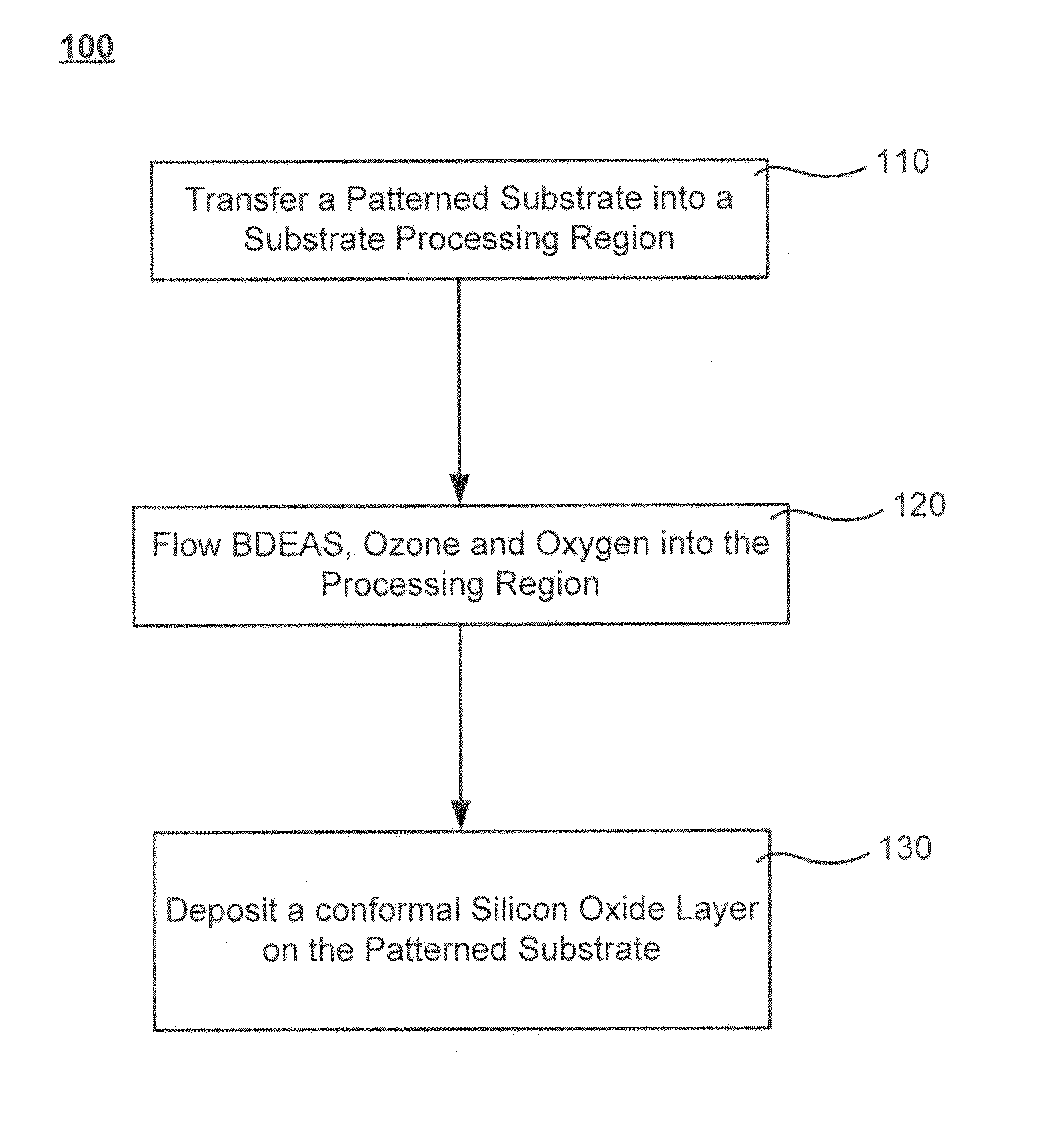
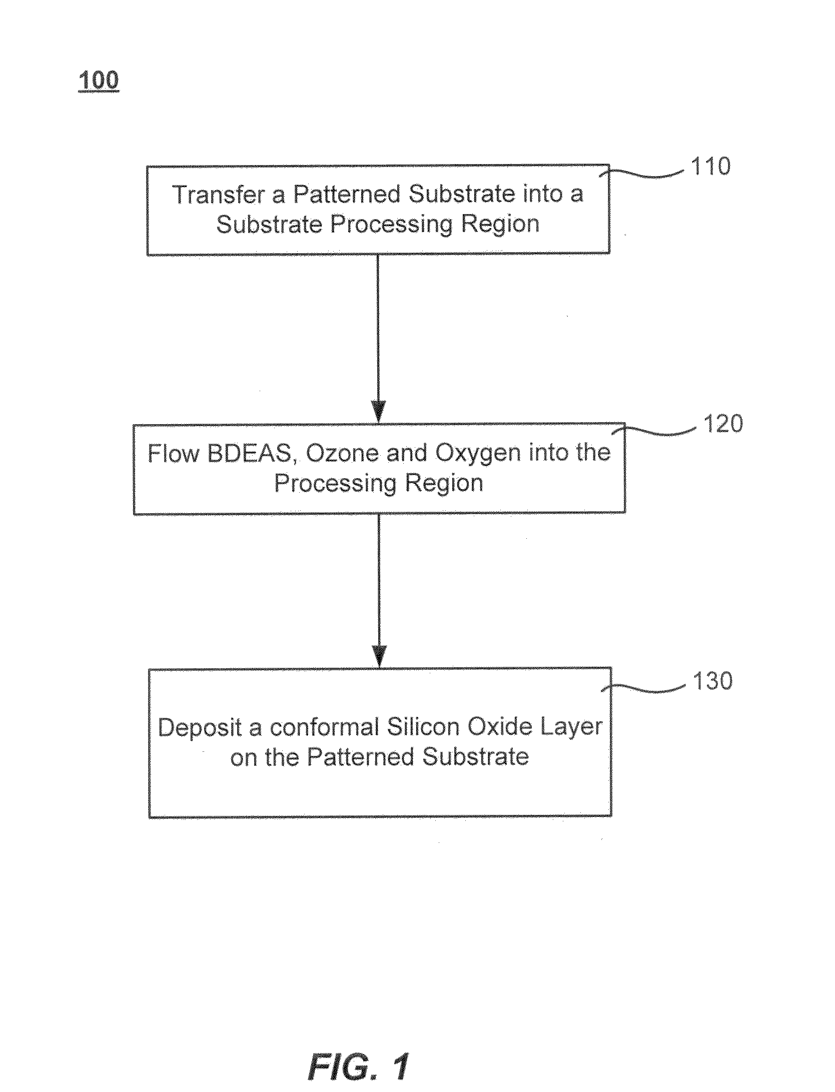
[0017]Aspects of the disclosure pertain to methods of depositing dielectric layers on patterned substrates. In embodiments, dielectric layers are deposited by flowing BIS(DIETHYLAMINO)SILANE (BDEAS), ozone and molecular oxygen into a processing chamber such that a relatively uniform dielectric growth rate is achieved across the patterned substrate surface. The deposition of dielectric layers grown according to embodiments may have a reduced dependence on pattern density while still being suitable for non-sacrificial applications.

[0018]Embodiments of the invention are directed to methods of forming silicon oxide on a patterned surface of a substrate. Sub-atmospheric CVD (SACVD) and related processes involve flowing a silicon-containing precursor and an oxidizing precursor into a processing chamber to form silicon oxide on the substrate. The silicon-containing precursor may include TEOS and the oxidizing precursor may include ozone (O3), oxygen (O2) and / or oxygen radicals. The invento...


PUM

PropertyMeasurementUnit
pressureaaaaaaaaaa
temperatureaaaaaaaaaa
areaaaaaaaaaaa

Abstract

Aspects of the disclosure pertain to methods of depositing dielectric layers on patterned substrates. In embodiments, dielectric layers are deposited by flowing BIS(DIETHYLAMINO)SILANE (BDEAS), ozone and molecular oxygen into a processing chamber such that a relatively uniform dielectric growth rate is achieved across the patterned substrate surface. The deposition of dielectric layers grown according to embodiments may have a reduced dependence on pattern density while still being suitable for non-sacrificial applications.

Description

CROSS-REFERENCES TO RELATED APPLICATIONS[0001]This application claims the benefit of U.S. Prov. Pat. App. No. 61 / 311,949 filed Mar. 9, 2010, and titled “REDUCED PATTERN LOADING USING BIS(DIETHYLAMINO)SILANE (C8H22N2Si) AS SILICON PRECURSOR,” which is incorporated herein by reference for all purposes.FIELD[0002]This application relates to manufacturing technology solutions involving equipment, processes, and materials used in the deposition, patterning, and treatment of thin-films and coatings, with representative examples including (but not limited to) applications involving: semiconductor and dielectric materials and devices, silicon-based wafers and flat panel displays (such as TFTs).BACKGROUND OF THE INVENTION[0003]Forming dielectric layers on a substrate by chemical reaction of gases is one of the primary steps in the fabrication of modern semiconductor devices. These deposition processes include chemical vapor deposition (CVD) as well as plasma enhanced chemical vapor depositio...

Claims


Application Information

Patent Timeline
Patent Type & Authority Applications(United States)
IPC IPC(8): H01L21/316
CPCC23C16/401H01L21/02271H01L21/02219H01L21/02164
Inventor KWESKIN, SASHAGEE, PAUL EDWARDVENKATARAMAN, SHANKARSAPRE, KEDAR
Owner APPLIED MATERIALS INC
Why Eureka
Try Eureka