Power-up circuit

Active Publication Date: 2011-09-22
ELITE SEMICON MEMORY TECH INC
View PDF14 Cites 0 Cited by
  • Summary
  • Abstract
  • Description
  • Claims
  • Application Information

AI Technical Summary

Benefits of technology

[0008]An aspect of the present invention is to provide a power-up circuit, and mo

Problems solved by technology

Although the conventional RC time delay circuit is generally suitable to provide a power-up signal, it is problematic in the case of a slow-rising supply voltage.
When the supply voltage ramps up relatively slowly compared with the charging rate of the capacitor, the power-up pulse may not be generated, and power-up failure will occur.
Because the detection signals PUPB1, PUPB2 are independent from each other, this circuit may have a problem with various supply voltage rising sequences.

Method used


Image

  • Power-up circuit
  • Power-up circuit
  • Power-up circuit

Examples


Embodiment Construction

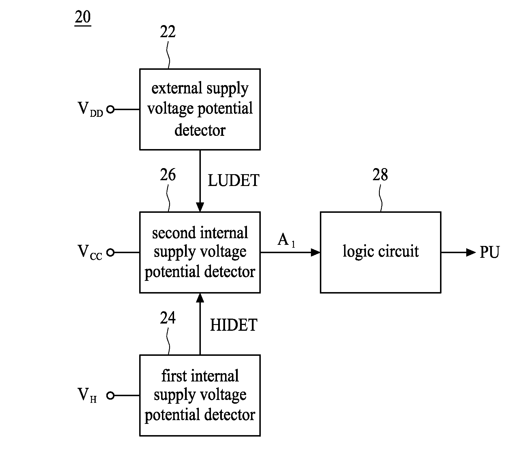
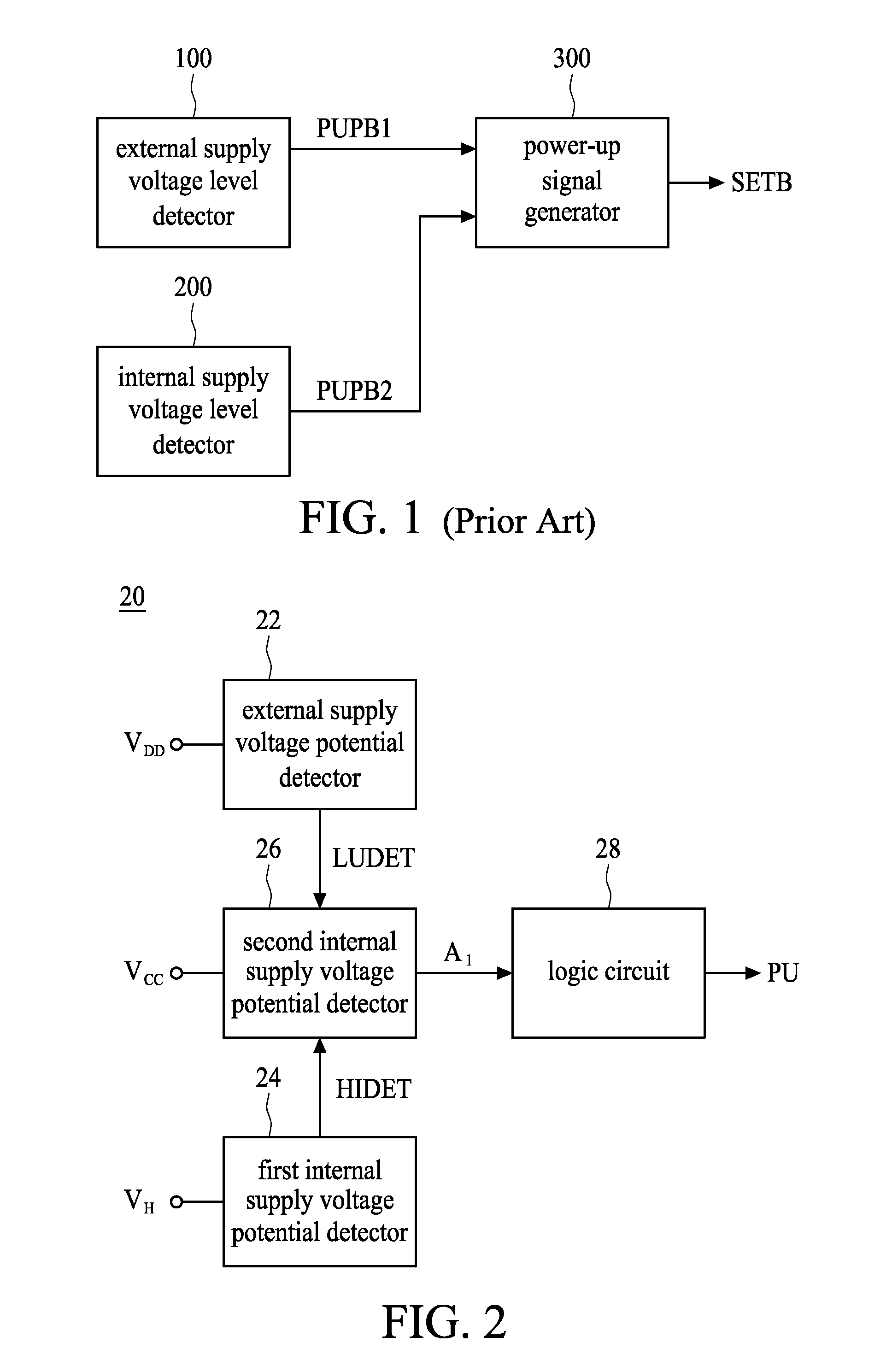
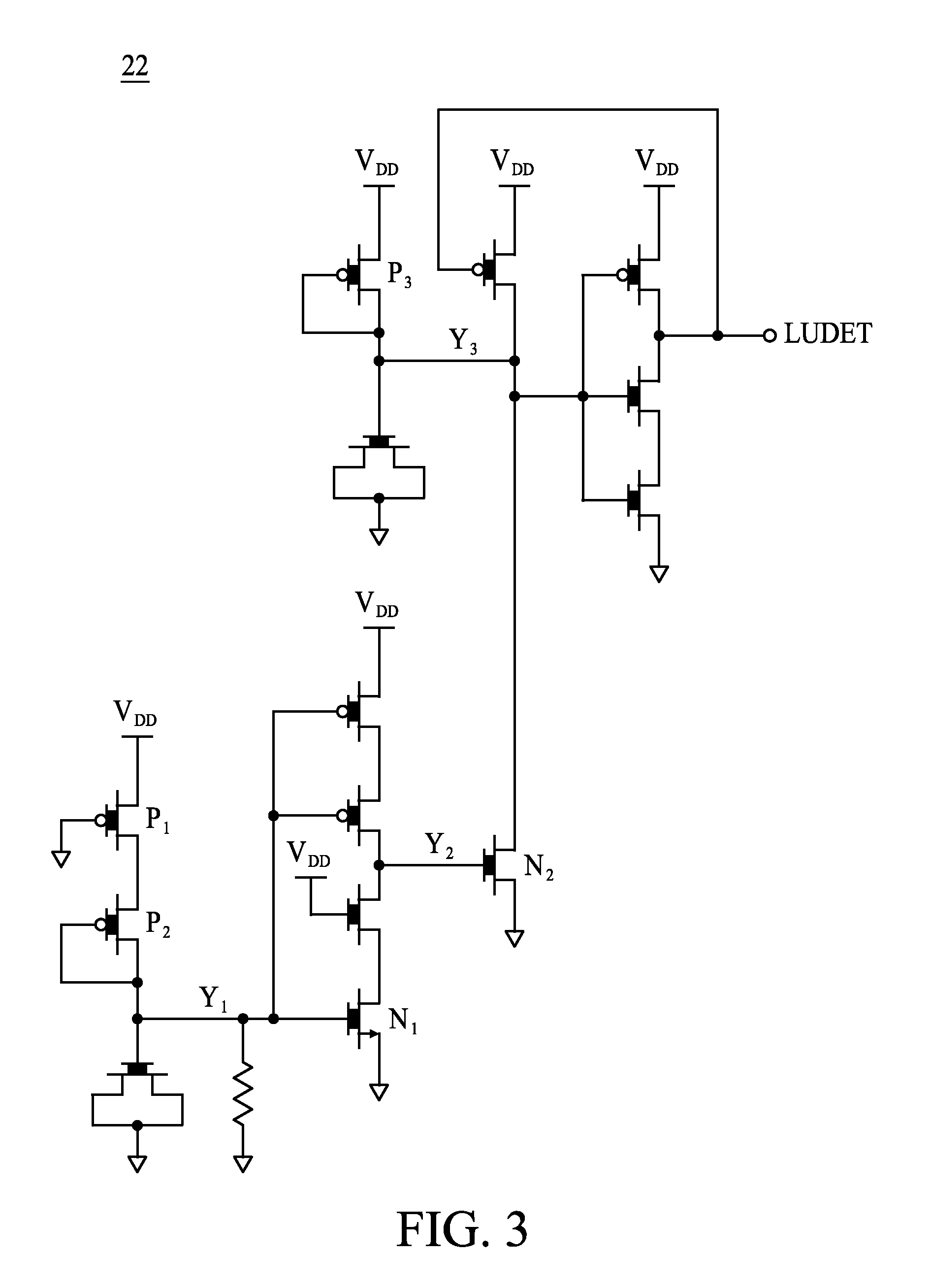
[0018]FIG. 2 shows a block diagram of a power-up circuit 20 for a semiconductor memory device according to one embodiment of the present invention. The power-up circuit 20 comprises an external supply voltage potential detector 22, a first internal supply voltage potential detector 24, a second internal supply voltage potential detector 26, and a logic circuit 28. Referring to FIG. 2, the external supply voltage potential detector 22 is configured to detect an external supply voltage VDD that is external to the memory device (not shown) and to generate a detection signal LUDET, and the first internal supply voltage potential detector 24 is configured to detect an internal supply voltage VH that is internal to the memory device and to generate a second detection signal.

[0019]The second internal supply voltage potential detector 26 is configured to detect an internal supply voltage VCC that is internal to the memory device and to receive the detection signal LUDET and an output voltag...


PUM


Abstract

A power-up circuit comprises an external supply voltage potential detector, a first internal supply voltage potential detector, a second internal supply voltage potential detector, and a logic circuit. The external supply voltage potential detector is configured to detect a supply voltage that is external to the memory device and to generate a first detection signal indicating whether a voltage potential of the external supply voltage reaches a first predetermined value. The first internal supply voltage potential detector is configured to detect a first internal supply voltage that is internal to the memory device and to generate a second detection signal indicating whether a voltage potential of the first internal supply voltage reaches a second predetermined value. The second internal supply voltage potential detector is configured to detect a second internal supply voltage that is internal to the memory device and to receive the first detection signal and an output voltage of the first internal supply voltage potential detector for generating a third detection signal indicating whether the voltage potentials of the external supply voltage and the first and second internal supply voltages reach the first, second, and third predetermined values respectively. The logic circuit is configured to receive the third detection signal and to generate a power-up signal.

Description

BACKGROUND OF THE INVENTION[0001]1. Field of the Invention[0002]The present invention relates to a power-up circuit, and more particularly, to a power-up circuit for a semiconductor memory device.[0003]2. Description of the Related Art[0004]Power-up circuits are often included in integrated circuit chips for providing a power-up pulse that initializes the different portions of the circuit when a supply voltage is applied to the chip. For example, in a computer system, many electronic devices in the system, such as a memory device, need to be driven to an initial condition prior to being used after the computer system is turned on or reset. A typical memory device has memory cells which use a variety of logic circuits such as latches and flip-flops to support their operation. These logic circuits need to be driven to an initial condition before the memory device is used to store data. As such, a power-up circuit is used to ensure that the logic circuits are initialized without floati...

Claims


Application Information

Patent Timeline
IPC IPC(8): G11C5/14
CPCG11C5/147G11C5/143
Inventor CHEN, CHUNG ZEN
Owner ELITE SEMICON MEMORY TECH INC
Why Eureka
Try Eureka