Method of Patterning an Electronig of Photonic Material
a photonic material and electronigmatic technology, applied in the association of printed electric components, printed circuit non-printed electric components, printed circuit manufacturing, etc., can solve the problems of low onoff current ratio of transistors, undesirable crosstalk in the realization of integrated circuits, and difficulty in avoiding compromises and trade-offs, so as to reduce any disruption to the physical microstructure of the layer
- Summary
- Abstract
- Description
- Claims
- Application Information
AI Technical Summary
Benefits of technology
Problems solved by technology
Method used
Image
Examples
example 1
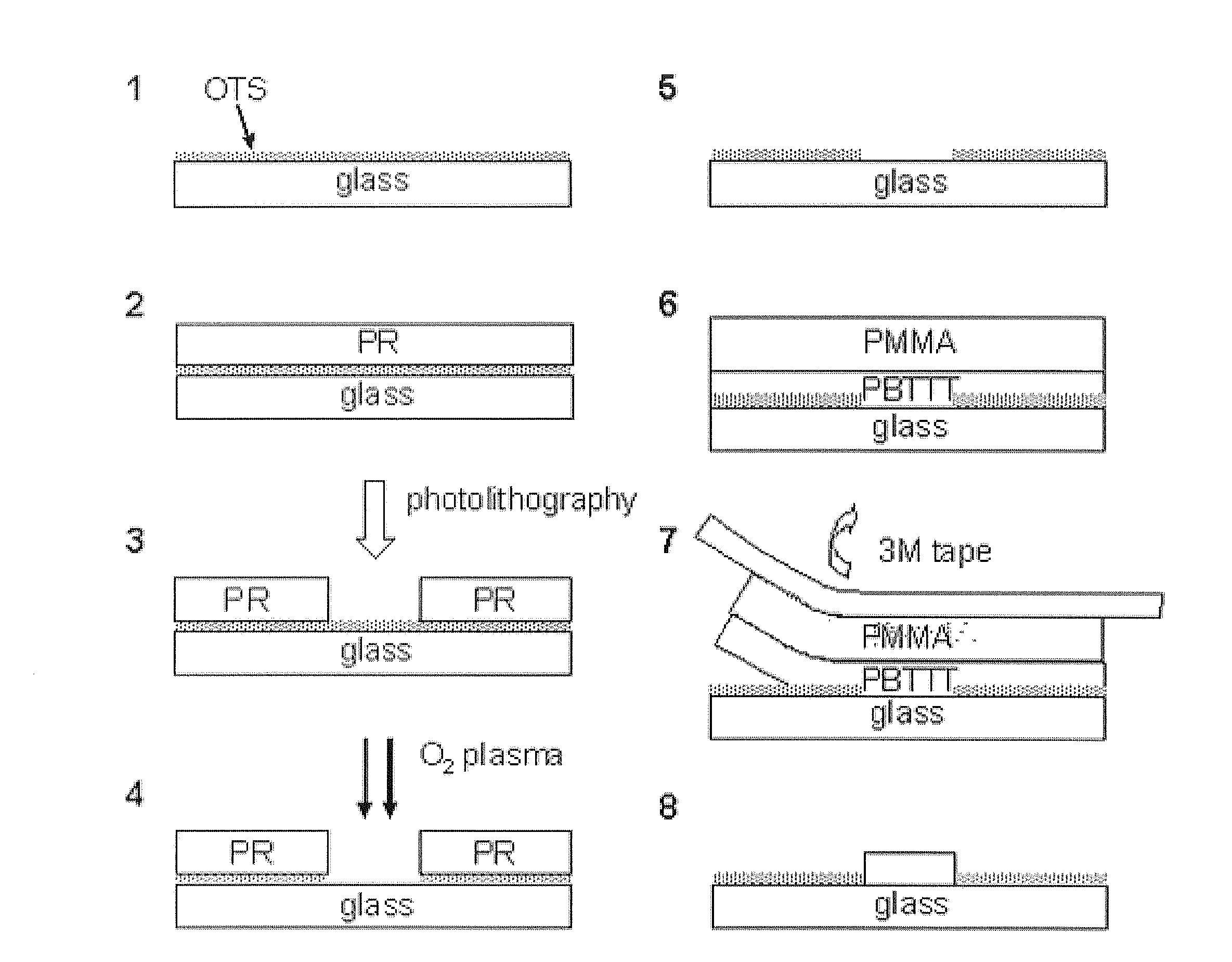
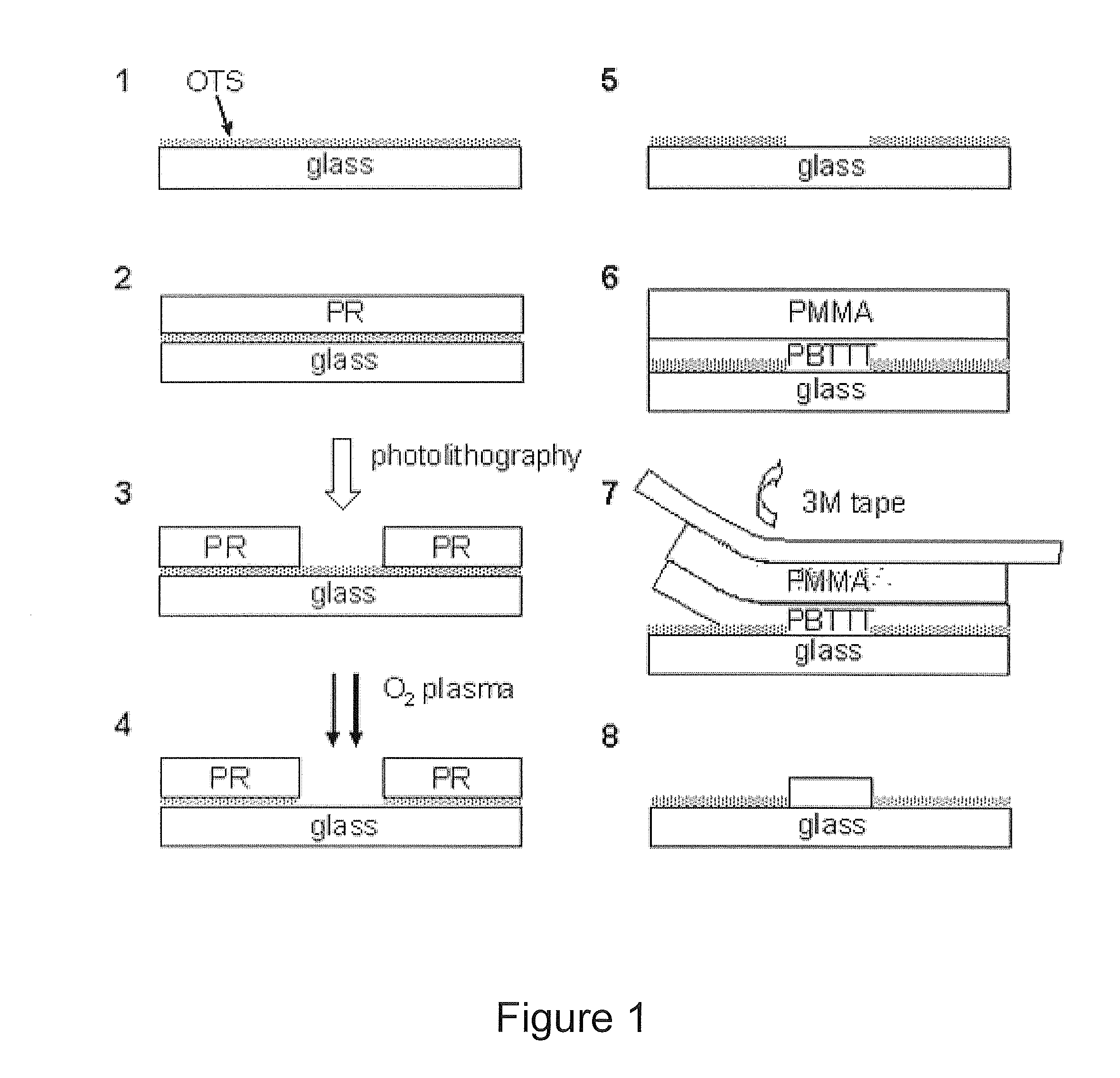
[0054]The process of a first embodiment as illustrated in FIG. 1 was followed. Octyltrichlorosilane (OTS) was deposited as a self-assembled monolayer on a bare glass substrate. The OTS layer was then patterned with conventional photolithography to create a lateral contrast in surface energy. The OTS on the unprotected areas was removed with O2 plasma etching and the area became hydrophilic, whereas the areas covered with photoresist remained hydrophobic. After stripping the photoresist, a PBTTT thin film was spun, followed by spin-coating a poly(methylmethacrylate) (PMMA) film as a sacrificial layer. Finally, 3M Scotch tape was used to delaminate the PMMA films. Because the adhesion between PBTTT and PMMA films is stronger than the adhesion of PBTTT to the OTS-treated areas but weaker than the adhesion of PBTTT to the hydrophilic areas, the delamination of the PMMA film only peeled off the PBTTT film from the hydrophobic areas but left the PBTTT film only on the hydrophilic areas.
[0...
example 2
[0058]In the following a related embodiment that allows semi conducting polymers to be patterned on hydrophobic surfaces is presented. This method utilizes a patterned solid film as a sacrificial layer to peel off the semi conducting polymer film from the undesired areas on the substrate. Polyimide is chosen as the sacrificial layer because (i) it is sufficiently mechanically robust after being annealed, (ii) it can easily be patterned, and (iii) it can easily be delaminated from hydrophobic surfaces. The whole process is described in FIG. 4. An HMDS monolayer was deposited on a Si / Si02 substrate and then a polyimide film was spun with a thickness of −1 pm. The polyimide film was dried at 100° C. for 10 min and then annealed at 270° C. for 15-20 min. The resulting polyimide film can be dissolved in Shipley MF319 developer used in photolithography but not in the organic solvents used for the successive PBTTT deposition. After patterning the polyimide film, the HMDS monolayer was remo...
PUM
| Property | Measurement | Unit |
|---|---|---|
| Fraction | aaaaa | aaaaa |
| Thickness | aaaaa | aaaaa |
| Dielectric polarization enthalpy | aaaaa | aaaaa |
Abstract
Description
Claims
Application Information


