Photovoltaic structures produced with silicon ribbons

a technology of photovoltaic structures and silicon ribbons, applied in the field of photovoltaic devices, can solve the problems of less desirable non-renewable energy sources

Inactive Publication Date: 2011-10-20
NANOGRAM
View PDF0 Cites 14 Cited by
  • Summary
  • Abstract
  • Description
  • Claims
  • Application Information

AI Technical Summary

Benefits of technology

[0005]In one aspect, the invention pertains to a silicon ribbon processing apparatus. The silicon ribbon processing apparatus comprises a silicon ribbon production system, a deposition unit and a silicon ribbon handling system. The silicon ribbon production system generally comprises a crucible for holding a quantity of molten silicon and strings passing through the crucible to pull a silicon ribbon from the surface of molten silicon within the crucible. The deposition unit comprises a deposition element positioned to deposit a quantity of composition onto a moving silicon ribbon pulled from the silicon ribbon production system and a quantity of a composition to be deposited onto a surface of the silicon ribbon. Also, the silicon ribbon handling system generally comprises conveying elements positioned to control the movement of the silicon ribbon from the silicon ribbon production unit past the deposition unit.

Problems solved by technology

With non-renewable energy sources continuing to be less desirable due to environmental and cost concerns, there is continuing interest in alternative energy sources, especially renewable energy sources.

Method used


Image

  • Photovoltaic structures produced with silicon ribbons
  • Photovoltaic structures produced with silicon ribbons
  • Photovoltaic structures produced with silicon ribbons

Examples


Embodiment Construction

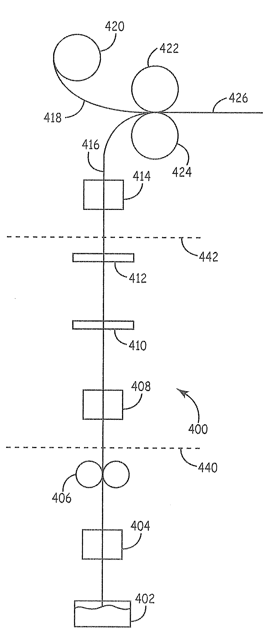
[0025]As described herein, efficient manufacturing of solar cells and modules can be accomplished using silicon ribbons for a silicon semiconductor core of the cells. Silicon ribbons provide a cost effective source of silicon that can be produced with good qualities. Silicon ribbons are polycrystalline silicon sheets pulled from a molten silicon reservoir. Production techniques have been refined such that the silicon can be produced with relatively large crystallite size, such that the resulting solar cells can exhibit good efficiencies. Processes with some processing steps and / or stabilization of the silicon while the ribbon remains on the move from initial formation can simplify the overall process and facilitate formation of lower cost photovoltaic cells. In some embodiments, low temperature process steps can be used to form the solar cells for corresponding energy savings during cell production. In additional or alternative embodiments, processing steps can be performed on the r...


PUM

PropertyMeasurementUnit
temperatureaaaaaaaaaa
thicknessaaaaaaaaaa
widthaaaaaaaaaa

Abstract

Photovoltaic elements can be formed by in-motion processing of a silicon ribbon. In some embodiments, only a single surface of a silicon ribbon is processed in-motion. In other embodiments both surfaces of a silicon ribbon is processed in-motion. In-motion processing can include, but is not limited to, formation of patterned or uniform doped regions within or along the silicon ribbon as well as the formation of patterned or uniform dielectric layers and/or electrically conductive elements on the silicon ribbon. After performing in-motion processing, additional processing steps can be performed after the ribbon is cut into portions. Furthermore, post-cut processing can include, but is not limited to, the formation of solar cells, photovoltaic modules, and solar panels.

Description

CROSS REFERENCE TO RELATED APPLICATIONS[0001]This application claims priority to copending U.S. provisional patent application Ser. No. 61 / 262,273 filed Nov. 18, 2009 to Chiruvolu et al., entitled “Photovoltaic Structures Assembled form Silicon Ribbons,” incorporated herein by reference.FIELD OF THE INVENTION[0002]The invention relates to photovoltaic devices comprising sheets of elemental silicon as the light receiving material that generates a photocurrent with doped structures used for harvesting the photocurrent. The invention further relates to methods for directly processing silicon ribbons as the ribbons are being generated to form structures relevant for the photovoltaic element.BACKGROUND OF THE INVENTION[0003]Photovoltaic cells operate through the absorption of light to form electron-hole pairs. A semiconductor material can be conveniently used to absorb the light with a resulting charge separation. The photocurrent is harvested at a voltage differential to perform useful ...

Claims


Application Information

Patent Timeline
Patent Type & Authority Applications(United States)
IPC IPC(8): B32B9/00H01L21/225B32B37/00B05C5/00C23C16/00H01L21/31B05B13/02
CPCC30B15/007C30B15/04C30B15/24C30B25/00Y02E10/547H01L31/042H01L31/048H01L31/1804H01L31/1868C30B29/06Y02P70/50
Inventor CHIRUVOLU, SHIVKUMARPAKALA, NEERAJFERGUSON, SCOTTDRAIN, KIERAN
Owner NANOGRAM
Why Eureka
Try Eureka