Method of Manufacturing Semiconductor Devices
Inactive Publication Date: 2011-10-27
SK HYNIX INC
3 Cites 5 Cited by
AI-Extracted Technical Summary
Problems solved by technology
Accordingly, a void or seam is generated within the contact hole or the trench, making it gradually more difficult to perform the gap-fill process.
Such etch damage may cause an increase in t...
Benefits of technology
[0009]An exemplary embodiment prevents the generation of voids d...
Abstract
A method of manufacturing semiconductor devices includes forming a dielectric interlayer over a semiconductor substrate, wherein a wet etch rate (WER) is faster in an upper part of the dielectric interlayer than in a lower part of the dielectric interlayer, forming trenches in the dielectric interlayer, performing a cleaning process to make a width of an opening portion in an upper part of each of the trenches wider than a width of an opening portion in lower part of the trench, and filling the trenches with a metal layer.
Application Domain
Semiconductor/solid-state device manufacturing
Technology Topic
Etching rateEngineering +2
Image
Examples
- Experimental program(1)
Example
[0022]Hereinafter, an exemplary embodiment of the disclosure is described in detail with reference to the accompanying drawings. The drawing figures are provided to allow those having ordinary skill in the art to understand the scope of the embodiment of the disclosure.
[0023]FIGS. 2A to 2G are cross-sectional views illustrating a method of manufacturing semiconductor devices according to an exemplary embodiment of this disclosure.
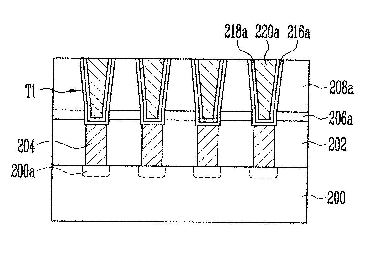
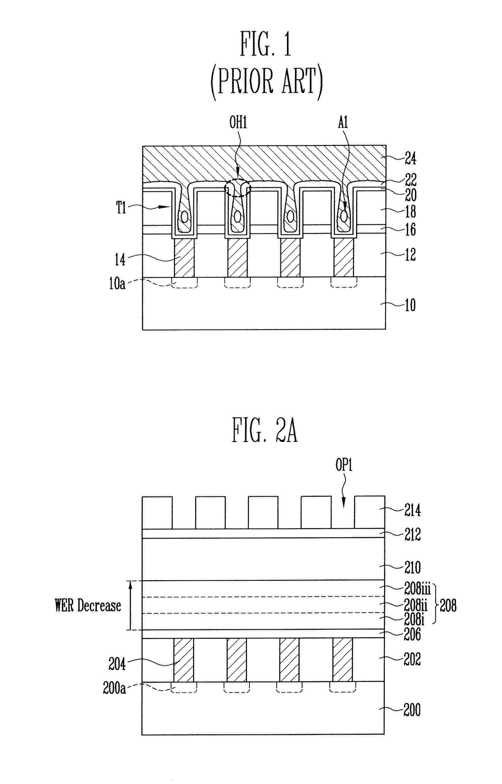
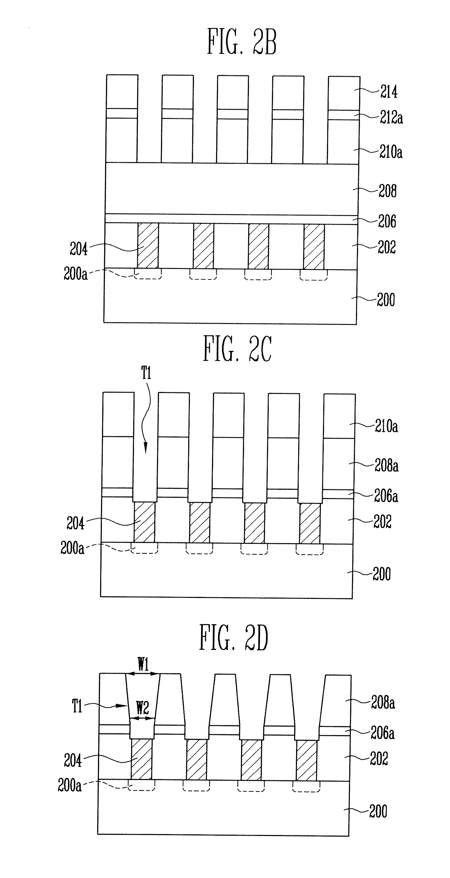
[0024]Referring to FIG. 2A, a first dielectric interlayer 202 and contact plugs 204 are formed over a semiconductor substrate 200 having junctions 200a formed therein. Preferably, the first dielectric interlayer 202 is formed on the semiconductor substrate 200. After contact holes are formed in the first dielectric interlayer 202 to expose the junctions 200a, the contact holes are filled with a metal material to form the contact plugs 204.
[0025]An etch-stop layer 206, a second dielectric interlayer 208, a hard mask layer 210, and a bottom anti-reflective coating layer 212 are formed over the first dielectric interlayer 202 and the contact plugs 204. Photoresist patterns 214 having opening portions OP1 formed therein are formed over the bottom anti-reflective coating layer 212. Here, the opening portions OP1 are formed in respective areas in which trenches will be formed.
[0026]The etch-stop layer 206 preferably is formed of a nitride layer, and the second dielectric interlayer 208 preferably is formed of a plasma-enhanced tetra ethyl ortho silicate (PE-TEOS) layer. The hard mask layer 210 preferably is formed of an amorphous carbon layer (ACL), and the bottom anti-reflective coating layer preferably is formed of an SiON layer.
[0027]In particular, the second dielectric interlayer 208 preferably has a wet etch rate (WER) that increases from the bottom to the top of the second dielectric interlayer. Thus, in the same etch process, the wet etch rate (WER) is faster in the upper part of the second dielectric interlayer 208 than in a lower part of the second dielectric interlayer 208. This can be achieved by differently forming the physical properties of the second dielectric interlayer 208 according to the height.
[0028]More particularly, a method of forming the second dielectric interlayer 208 is described as follows, with reference to FIG. 3, which is a graph illustrating the wet etch rate (WER) according to deposition process conditions for the dielectric interlayer using a well-known showerhead-type reactor, wherein reactant gases (e.g., O2) are passed at variable rates through a showerhead distributor that is spaced by a variable interval from a substrate under application of variable power (e.g., RF power).
[0029]Where the second dielectric interlayer 208 is formed of a plasma-enhanced tetra ethyl ortho silicate (PE-TEOS) layer or an SiO2 layer, for example, in a deposition process, the wet etch ratio (WER) may be increased with a decrease in applied RF power and/or the flow rate of O2 or with an increase of the size of the interval between the semiconductor substrate 200 and the shower head (that is, the distributor head through which reactant gas is injected within a chamber). On the other hand, in a deposition process, the wet etch ratio (WER) may be decreased with an increase in the RF power and/or the flow rate of O2 or with a decrease in the size of the interval between the semiconductor substrate 200 and the shower head.
[0030]In this disclosure, the wet etch ratio (WER) preferably increased from the bottom of the second dielectric interlayer 208 to the top thereof. Thus, the wet etch rate (WER) is faster in the upper part of the second dielectric interlayer 208 than in the lower part of the second dielectric interlayer 208. To this end, the deposition process preferably performed using one of three methods: a method of gradually decreasing the RF power, a method of gradually decreasing the flow rate of O2, and a method of gradually increasing the size of the interval between the semiconductor substrate and the shower head, or a combination of any of the three methods. In particular, if the three methods are used at the same time, the wet etch ratio (WER) can be increased at least three times or more as compared to when other process conditions.
[0031]Alternatively, the second dielectric interlayer 208 may be formed in such a manner that the second dielectric interlayer 208 is divided into a number of sections and process conditions are changed for every section. For example, in the case where the final thickness of the second dielectric interlayer 208 is divided into three sections, a second dielectric interlayer first section 208i may be formed in a thickness equal to ⅓ of a target thickness, in the first section over the etch-stop layer 206. Next, a second dielectric interlayer second section 208ii may be formed in a thickness in the second section so that the sum of the thicknesses of the second dielectric interlayer first and second sections 208i and 208ii is equal to ⅔ of the target thickness. Next, a second dielectric interlayer third section 208iii may be formed in ⅓ of the target thickness.
[0032]Here, the RF power preferably is decreased more in the second section 208ii than in the first section 208i, the flow rate of O2 preferably is decreased more in the second section 208ii than in the first section 208i, and the size of the interval between the semiconductor substrate and the shower head preferably is increased more in the second section 208ii than in the first section 208i so that the second dielectric interlayer second section 208ii has a lower wet etch ratio (WER) than the second dielectric interlayer first section 208i.
[0033]Furthermore, the RF power preferably is decreased more in the third section 208iii than in the second section 208ii, the flow rate of O2 preferably is decreased more in the third section 208iii than in the second section 208ii, and the size of the interval between the semiconductor substrate and the shower head preferably is increased more in the third section 208iii than in the second section 208ii so that the second dielectric interlayer third section has a lower wet etch ratio (WER) than the second dielectric interlayer second section.
[0034]The second dielectric interlayer first to third sections 208i to 208iii preferably are formed using an in-situ method within the same reaction chamber. In some embodiments, a target thickness of the dielectric interlayer 208 may be divided into n (for example, four or more) sections, and the wet etch rate (WER) may be controlled according to the n divided sections.
[0035]Referring to FIG. 2B, a first etch process of patterning the bottom anti-reflective coating layer 212 and the hard mask layer 210 by using the photoresist patterns 214 as an etch mask is performed. Consequently, bottom anti-reflective coating patterns 212a and hard mask patterns 210a are formed.
[0036]Referring to FIG. 2C, after the photoresist patterns (refer to 214 of FIG. 2B) and the bottom anti-reflective coating patterns (refer to 212a of FIG. 2B) are removed, a second etch process using the hard mask patterns 210a as an etch mask is performed to pattern the second dielectric interlayer 208 and the etch-stop layer 206. Consequently, second interlayer insulating patterns 208a and etch-stop patterns 206a are formed and, at the same time, trenches T1 are formed in respective areas in which metal lines will be formed. The trenches T1 are formed to expose the respective contact plugs 204, and each of the trenches T1 preferably is wider than the contact plug 204 for an alignment margin.
[0037]Referring to FIG. 2D, after the hard mask patterns 210a are removed (refer to 210a of FIG. 2C), a cleaning process for removing residues that may remain on a surface of the second interlayer insulating patterns 208a is performed. The cleaning process preferably is performed using a wet etch process and preferably is performed using an etchant capable of removing an oxide layer. For example, the cleaning process preferably is performed using a buffered oxide etchant (BOE) or HF solution.
[0038]In particular, the second interlayer insulating patterns 208a preferably are also removed during the cleaning process. More particularly, since the upper part of the second interlayer insulating pattern 208a has a higher wet etch ratio (WER) than the lower part of the second interlayer insulating pattern 208a, the upper part of the second interlayer insulating pattern 208a is removed faster than the lower part thereof.
[0039]Accordingly, the width W1 of an opening portion in an upper part of the trench T1 becomes larger than the width W2 of an opening portion in a lower part of the trench T1. Here, a ratio of the width W1 and the width W2 of the opening portions can be controlled by adjusting the time that it takes to perform the cleaning process.
[0040]Referring to FIG. 2E, a barrier layer 216 and a seed layer 218 are formed on a surface of the second interlayer insulating patterns 208a, the etch-stop patterns 206a, and the exposed contact plugs 204. The barrier layer 216 is formed to prevent the diffusion of metal lines to be subsequently formed. The barrier layer 216 preferably is formed of any one of a titanium (Ti) layer, a tantalum (Ta) layer, a ruthenium (Ru) layer, a cobalt (Co) layer, a TiN layer, and a TaN layer. The seed layer 218 preferably is formed to facilitate the formation of a subsequent metal layer (refer to 220 of FIG. 2F). The barrier layer 216 and the seed layer 218 preferably are formed using a physical vapor deposition (PVD) method. Since the width W1 of an upper part of the trench T1 is larger than the width W2 of an lower part of the trench T1, an overhang can be prevented from being formed in an upper part of the second interlayer insulating pattern 208a, even if the barrier layer 216 and the seed layer 218 are formed using the physical vapor deposition (PVD) method.
[0041]Referring to FIG. 2F, a metal layer 220 for metal lines is formed over the seed layer 218 to fill the trenches T1. The metal layer 220 preferably is formed of copper (Cu) or tungsten (W). In particular, a void or seam is not generated in the trench T1 in the gap-fill process for filling the inside of the trench T1 because the width W1 of an upper part of the trench T1 is larger than the width W2 of a lower part of the trench T1 and an overhang resulting from the barrier layer 216 and the seed layer 218 is not generated on an upper part of the second interlayer insulating pattern 208a. The metal layer 220 preferably is formed in a thickness of 2000 Å to 10000 Å to sufficiently fill the inside of the trenches T1.
[0042]Referring to FIG. 2G, a chemical mechanical polishing (CMP) process or other suitable process is performed on the metal layer 220 so that the top surfaces of the second interlayer insulating patterns 208a are exposed. Consequently, a barrier pattern 216a, a seed pattern 218a, and a metal line 220a are formed within each of the trenches T1.
[0043]As described above, in the process of forming the second dielectric interlayer 208, the physical properties of the second dielectric interlayer 208 can be formed differently according to the height of the interlayer by changing process conditions. Accordingly, the width of an upper part of the trench T1 becomes larger than the width of a lower part of the trench T1 in the subsequent cleaning process, the subsequent gap-fill process for forming the metal layer 220 for the metal lines 220a can be easily performed.
[0044]In other words, since the generation of a void or seam within the trenches is prevented, an increase in the resistance of the metal lines 220a can be prevented. Accordingly, the electrical properties of semiconductor devices can be prevented from deteriorating.
[0045]This disclosure is not limited to the process of forming the metal lines described above, but may also be applied to a gap-fill process using a damascene process, for example.
[0046]As described above, according to the present disclosure, since the width of an upper part of a trench or a contact hole is formed to be larger than the width of a lower part of the trench or the contact hole, generation of a void or seam can be prevented in a gap-fill process. Accordingly, an increase in the resistance of metal lines or contact plugs can be prevented, and so the electrical properties of semiconductor devices can be prevented from deteriorating.
PUM


Description & Claims & Application Information
We can also present the details of the Description, Claims and Application information to help users get a comprehensive understanding of the technical details of the patent, such as background art, summary of invention, brief description of drawings, description of embodiments, and other original content. On the other hand, users can also determine the specific scope of protection of the technology through the list of claims; as well as understand the changes in the life cycle of the technology with the presentation of the patent timeline. Login to view more.