Backside illumination image sensor and image-capturing device

a backside illumination and image sensor technology, applied in picture signal generators, color televisions, television systems, etc., can solve the problem that the relationship between the aperture f number at the image forming optical system and the level of signals output from the backside illumination image sensor cannot be kept inta

Active Publication Date: 2011-11-17
NIKON CORP
View PDF7 Cites 123 Cited by
  • Summary
  • Abstract
  • Description
  • Claims
  • Application Information

AI Technical Summary

Benefits of technology

[0007]According to the present invention, the linearity representing the relationship between the aperture F number at the image forming optical system and the level of the signals output by the backside illumination image sensor can be maintained with ease.
[0015]According to the 8th aspect of the present invention, in the backside illumination image sensor according to the 7th aspect, it is preferred that the light shielding member is a barrier member disposed parallel to an optical axis of the on-chip lens; and an anti-reflection film is formed at a surface of the barrier member so as to prevent reflection of the passing light.

Problems solved by technology

However, since they are designed without fully taking into consideration the positional relationship between the backside illumination image sensor and the exit pupil of the image forming optical system, the linearity of the relationship between the aperture F number at the image forming optical system and the level of the signals output from the backside illumination image sensor cannot be kept intact, necessitating that correction be executed as part of exposure control, particularly at low F numbers.

Method used


Image

  • Backside illumination image sensor and image-capturing device
  • Backside illumination image sensor and image-capturing device
  • Backside illumination image sensor and image-capturing device

Examples


Embodiment Construction

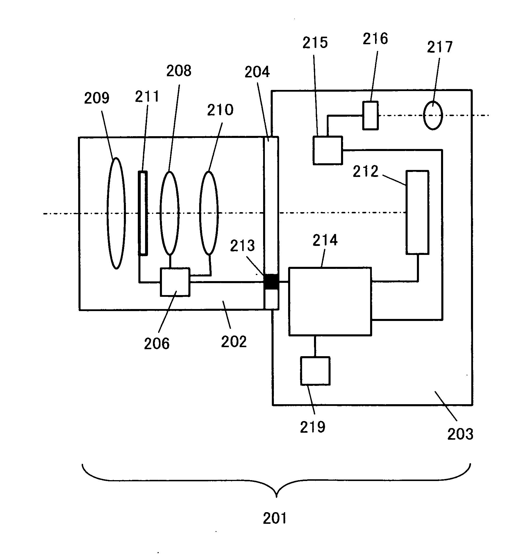
[0041]The following is a description of a digital still camera used in conjunction with interchangeable lenses, representing an example of an image-capturing device equipped with a backside illumination sensor (hereafter simply referred to as an “image sensor”) achieved in an embodiment of the present invention is now explained. FIG. 1 is a lateral sectional view of the structure adopted in the digital still camera in the embodiment. A digital still camera 201 achieved in the embodiment comprises an interchangeable lens 202 and a camera body 203. The interchangeable lens 202 is mounted at the camera body 203 via a mount unit 204. Namely, the interchangeable lens 202 that includes various image forming optical systems can be mounted at the camera body 203 via the mount unit 204.

[0042]The interchangeable lens 202 includes a a lens 209, a zooming lens 208, a focusing lens 210, an aperture 211, a lens drive control device 206 and the like. The lens drive control device 206 is constitute...


PUM


Abstract

A backside illumination image sensor that includes a semiconductor substrate with a plurality of photoelectric conversion elements and a read circuit formed on a front surface side of the semiconductor substrate, and captures an image by outputting, via the read circuit, electrical signals generated as incident light having reached a back surface side of the semiconductor substrate is received at the photoelectric conversion elements includes: a light shielding film formed on a side where incident light enters the photoelectric conversion elements, with an opening formed therein in correspondence to each photoelectric conversion element; and an on-chip lens formed at a position set apart from the light shielding film by a predetermined distance in correspondence to each photoelectric conversion element. The light shielding film and an exit pupil plane of the image forming optical system achieve a conjugate relation to each other with regard to the on-chip lens.

Description

INCORPORATION BY REFERENCE[0001]The disclosure of the following priority application is herein incorporated by reference: Japanese Patent Application No. 2010-040378 filed Feb. 25, 2010.BACKGROUND OF THE INVENTION[0002]1. Field of the Invention[0003]The present invention relates to a backside illumination image sensor and an image-capturing device.[0004]2. Description of Related Art[0005]The performance of an image sensor at low brightness is often improved by forming on-chip lenses, each in correspondence to one of the photoelectric conversion elements, and illuminating each photoelectric conversion element with condensed light. The backside illumination image sensor disclosed in Japanese Laid Open Patent Publication No. 2009-164385 captures an image as signals generated with light illuminating the back side of a semiconductor substrate, which is received at photoelectric conversion elements disposed in the semiconductor substrate, are output through a read circuit formed on the fr...

Claims


Application Information

Patent Timeline
Patent Type & Authority Applications(United States)
IPC IPC(8): H04N5/225
CPCH01L27/14621H01L27/14623H01L27/14627H04N5/3696H01L27/1464H01L27/14605H01L27/14625H01L27/1463H04N9/045H01L27/14645H01L27/1462H01L27/14643H04N23/63H04N25/702H04N25/134H04N25/75
Inventor KUSAKA, YOSUKE
Owner NIKON CORP
Why Eureka
Try Eureka