III-nitride switching device with an emulated diode

a switching device and nitride technology, applied in the direction of electronic switching, transistors, pulse techniques, etc., can solve the problems of difficult and complex integration of monolithic diodes in a gan hemt process, the adoption of monolithic integration into a single device is not yet as widespread in power conversion applications, and the zero reverse recovery characteristics further complicate the integration of monolithic devices into a single devi

Active Publication Date: 2011-11-24
INFINEON TECH AMERICAS CORP
View PDF17 Cites 47 Cited by
  • Summary
  • Abstract
  • Description
  • Claims
  • Application Information

AI Technical Summary

Benefits of technology

[0009]A III-nitride switching device with an emulated diode, substantially as shown in and/or ...

Problems solved by technology

Unfortunately, since the “intrinsic diode” is only the result of a silicon FET structure, III-nitride transistors require a separate diode to provide the same benefits as the “intrinsic diode” in silicon transistors.
However, integrating a monolithic diode in a GaN HEMT process is difficult and complex.
Moreover, for high performance switching applications, the need for Schottky-like diode perfor...

Method used


Image

  • III-nitride switching device with an emulated diode
  • III-nitride switching device with an emulated diode
  • III-nitride switching device with an emulated diode

Examples


Embodiment Construction

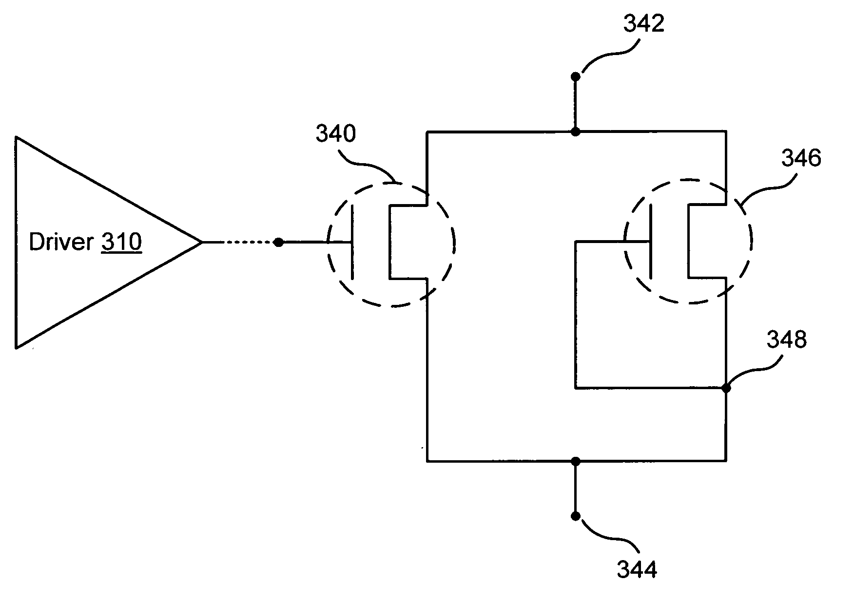
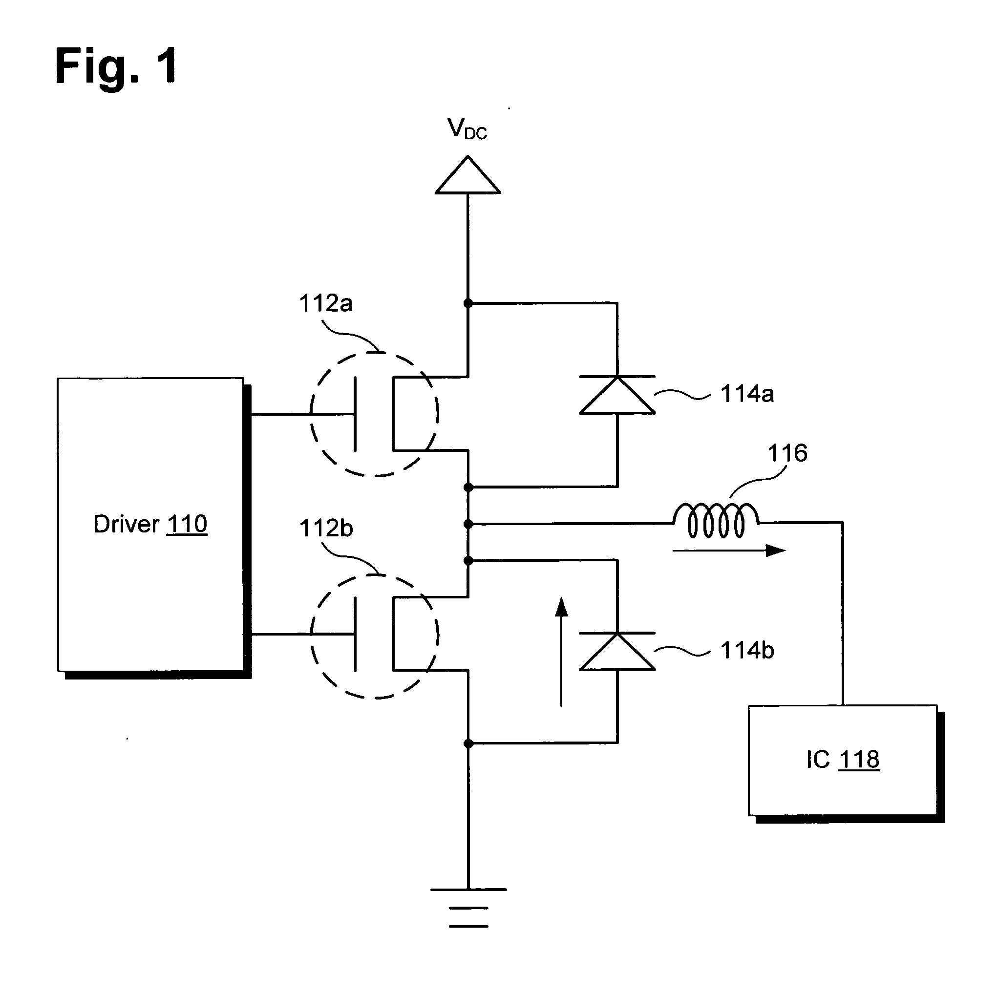
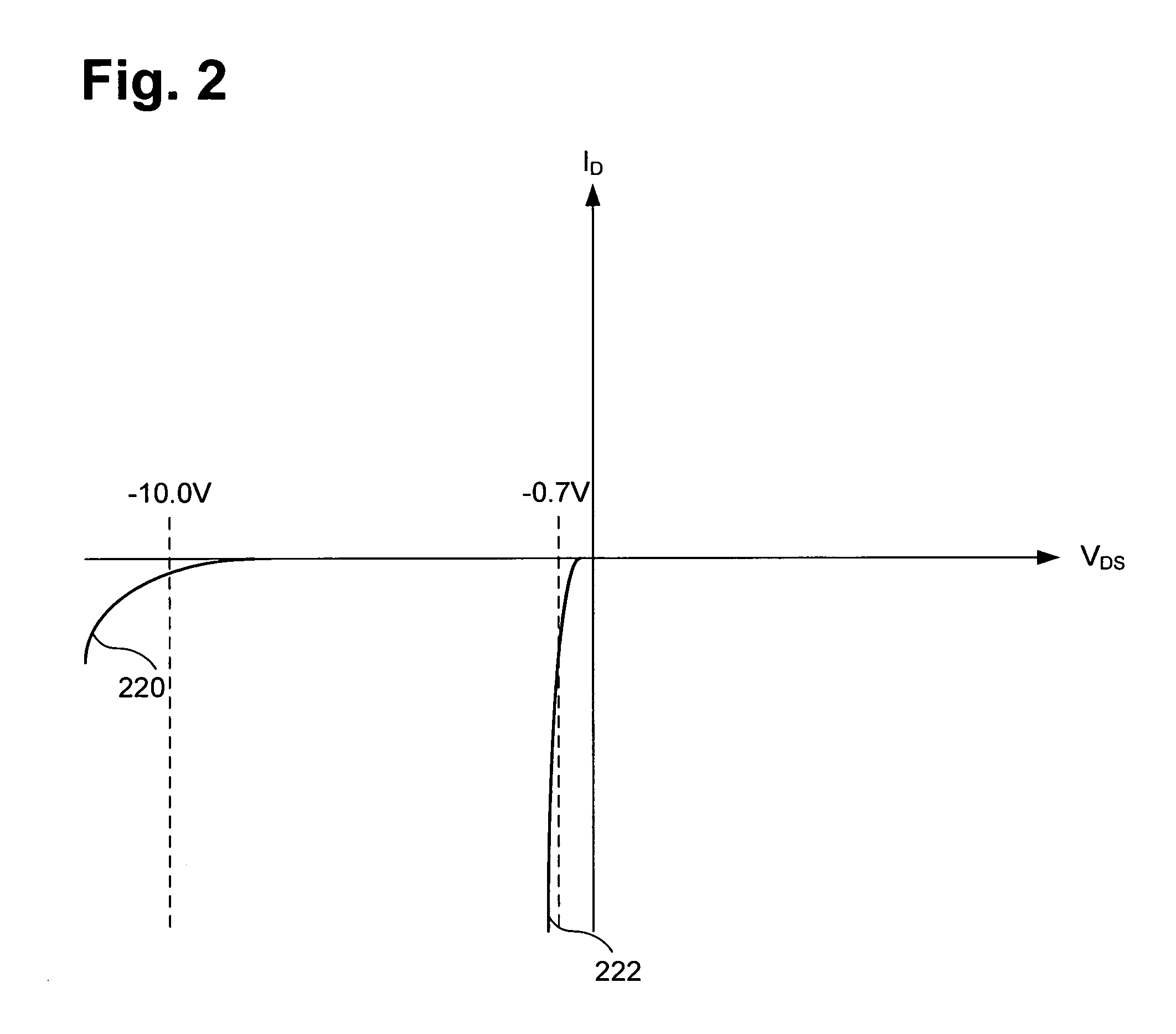
[0015]The present application is directed to a III-nitride switching device with an emulated diode. The following description contains specific information pertaining to the implementation of the present invention. One skilled in the art will recognize that the present invention may be implemented in a manner different from that specifically discussed in the present application. Moreover, some of the specific details of the invention are not discussed in order not to obscure the invention. The specific details not described in the present application are within the knowledge of a person of ordinary skill in the art.

[0016]The drawings in the present application and their accompanying detailed description are directed to merely exemplary embodiments of the invention. To maintain brevity, other embodiments of the invention, which use the principles of the present invention, are not specifically described in the present application and are not specifically illustrated by the present dra...


PUM


Abstract

Some exemplary embodiments of a III-nitride switching device with an emulated diode have been disclosed. One exemplary embodiment comprises a GaN switching device fabricated on a substrate comprising a high threshold GaN transistor coupled across a low threshold GaN transistor, wherein a gate and a source of the low threshold GaN transistor are shorted with an interconnect metal to function as a parallel diode in a reverse mode. The high threshold GaN transistor is configured to provide noise immunity for the GaN switching device when in a forward mode. The high threshold GaN transistor and the low threshold GaN transistor are typically fabricated on the same substrate, and with significantly different thresholds. As a result, the superior switching characteristics of III-nitride devices may be leveraged while retaining the functionality and the monolithic structure of the inherent body diode in traditional silicon FETs.

Description

DEFINITION[0001]In the present application, “III-nitride” refers to a compound semiconductor that includes nitrogen and at least one group III element, such as, but not limited to, GaN, AlGaN, InN, AlN, InGaN, InAlGaN and the like.BACKGROUND OF THE INVENTION[0002]1. Field of the Invention[0003]The present invention relates generally to transistors and switching circuits. More particularly, the present invention relates to III-nitride transistors and switching circuits.[0004]2. Background Art[0005]Silicon based transistors such as silicon metal-oxide-semiconductor field-effect transistors or MOSFETs may include the advantageous property of a body diode or an “intrinsic diode” due to their inherent silicon PN junctions. This “intrinsic diode” provides advantages such as inherent over-voltage (or under-voltage) protection for power conversion circuits without requiring a separate diode; thus reducing costs, improving efficiency, and simplifying circuit design.[0006]On the other hand, I...

Claims


Application Information

Patent Timeline
IPC IPC(8): H01L27/06H01L29/778H01L29/20
CPCH01L27/085H01L27/0605H01L21/8252H03K17/687H01L27/0255H01L27/0629H01L29/2003H01L29/205H01L29/7787H01L29/872
Inventor ZHANG, JASON
Owner INFINEON TECH AMERICAS CORP
Why Eureka
Try Eureka