Light-Emitting Device and Lighting Device

a technology of light-emitting devices and lighting devices, which is applied in the direction of semiconductor devices for light sources, lighting and heating apparatus, planar light sources, etc., can solve the problem of easy short circuit between the auxiliary wiring and the cathode of an el light-emitting element, and achieve the effect of high reliability

Active Publication Date: 2011-11-24
SEMICON ENERGY LAB CO LTD
View PDF3 Cites 10 Cited by
  • Summary
  • Abstract
  • Description
  • Claims
  • Application Information

AI Technical Summary

Benefits of technology

[0028]According to the present invention, a light-emitting device from which uniform light emission can be obtained can be provided. Moreover, a light-emitting device in which a short circuit between electrodes or between the electrode and an auxiliary wiring, which is attributed to a bump caused by the auxiliary wiring, is prevented can be provided. Furthermore, by preventing a short circuit, a highly reliable light-emitting device from which uniform light emission can be obtained can be provided.

Problems solved by technology

Thus, there has been a problem in that a short circuit between the auxiliary wiring and the cathode of an EL light-emitting element easily occurs due to a bump on side surfaces of the auxiliary wiring and the inorganic insulating layer.

Method used


Image

  • Light-Emitting Device and Lighting Device
  • Light-Emitting Device and Lighting Device
  • Light-Emitting Device and Lighting Device

Examples


embodiment 1

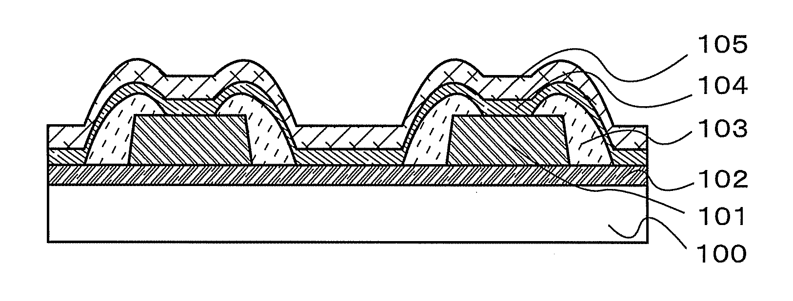
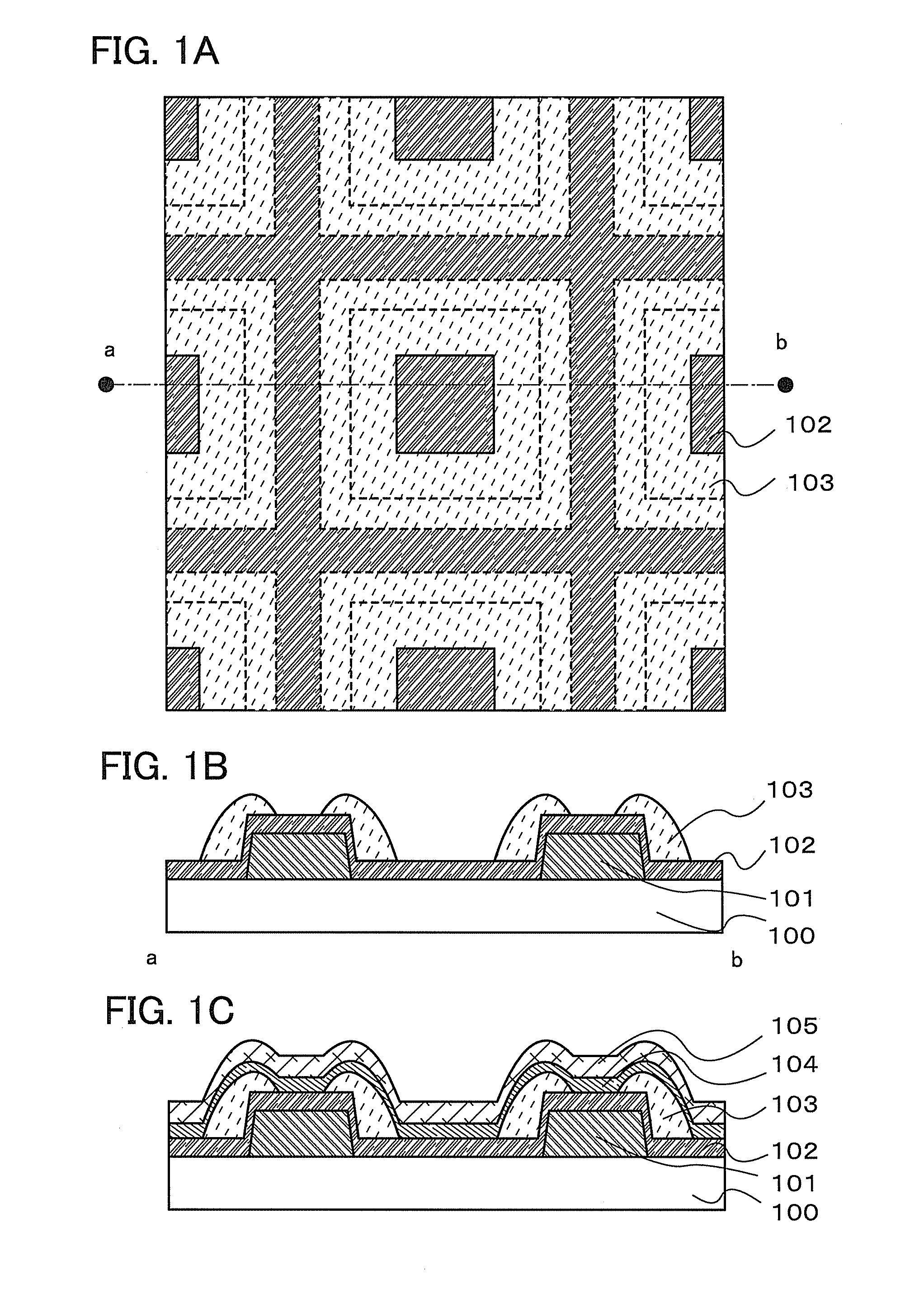
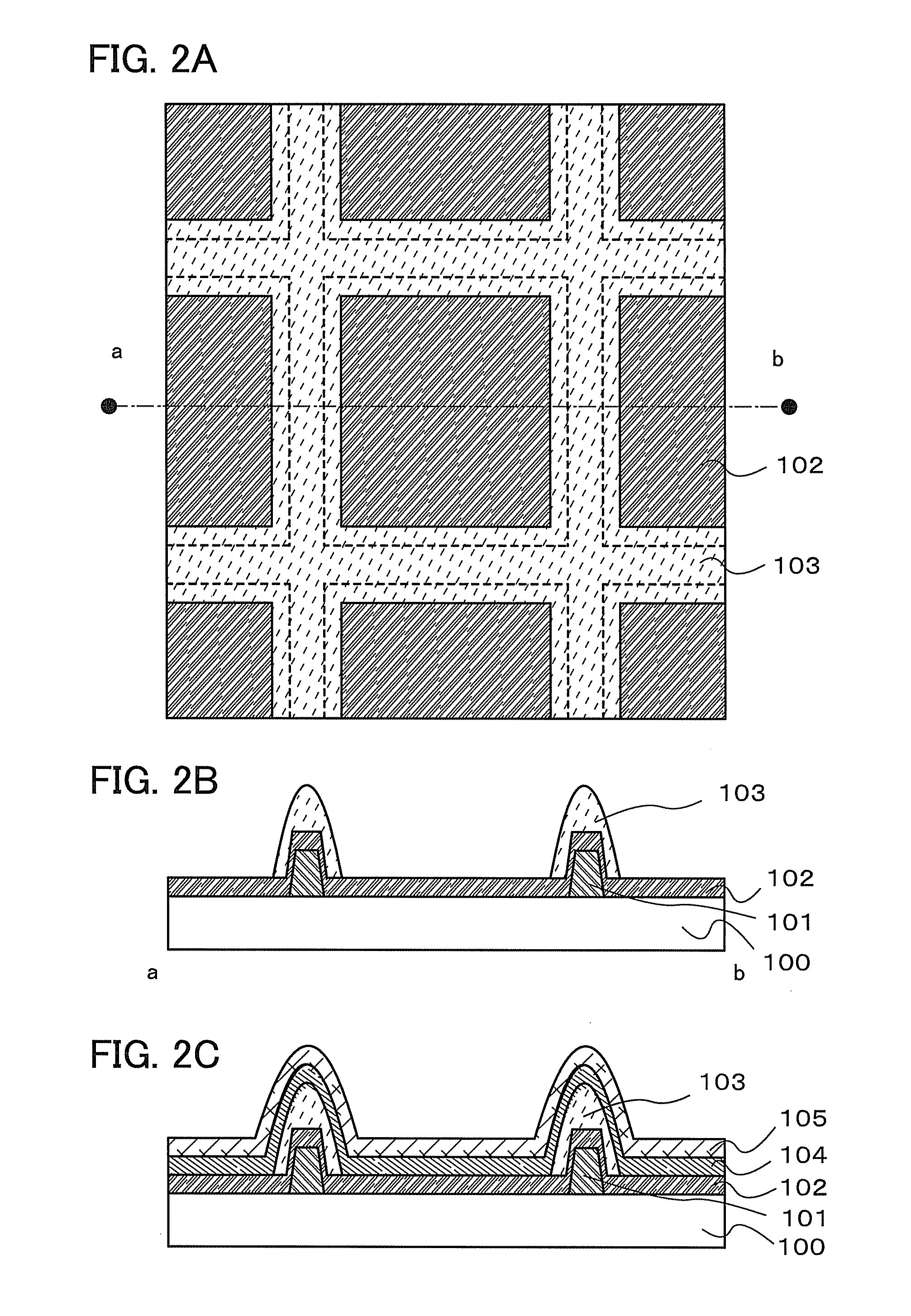
[0040]In this embodiment, a light-emitting device having a structure in which an auxiliary wiring is located under a first electrode and a bump of the first electrode, which is caused by the auxiliary wiring, is covered with an insulator will be described with reference to FIGS. 1A to 1C. Note that, although an example in which a substrate having an insulating surface is used as a mode of one having an insulating surface is described in this embodiment, the present invention is not limited thereto.

[0041]The light-emitting device described in this embodiment includes an auxiliary wiring 101 over a substrate 100, and a first electrode 102 which covers the substrate 100 and the auxiliary wiring 101. In addition, the light-emitting device includes an insulator 103 which covers a bump caused by the auxiliary wiring 101, over the first electrode 102. Furthermore, the light-emitting device includes an EL layer 104 which covers the first electrode 102 and the insulator 103, and a second ele...

embodiment 2

[0086]In this embodiment, a light-emitting device employing a structure in which an auxiliary wiring is formed over a first electrode and a bump caused by the auxiliary wiring is covered with an insulator will be described with reference to FIG. 7.

[0087]The light-emitting device described in this embodiment includes the first electrode 102 over the substrate 100, and the auxiliary wiring 101 over the first electrode 102. Moreover, the light-emitting device includes the insulator 103 which covers a bump caused by the auxiliary wiring 101. Furthermore, the light-emitting device includes the EL layer 104 which covers the auxiliary wiring 101, the first electrode 102, and the insulator 103, and the second electrode 105 over the EL layer 104.

[0088]The description in Embodiment 1 can be applied to components described in this embodiment; therefore, repetitive description is omitted in detailed description of each component.

[0089]In the structure to which this embodiment is applied, the bu...

embodiment 3

[0093]In this embodiment, light-emitting devices in which the insulators described in Embodiments 1 and 2 are formed by a wet process will be described with reference to FIGS. 9A and 9B.

[0094]FIG. 9A illustrates the light-emitting device described in Embodiment 1, which has a structure in which the auxiliary wiring 101 is formed over the substrate 100, the first electrode 102 for covering the substrate 100 and the auxiliary wiring 101 is formed, and the insulator 103 for covering a bump caused by the auxiliary wiring 101 is formed over the first electrode 102. In FIG. 9A, in particular, an edge of the auxiliary wiring 101 is perpendicular to the substrate. FIG. 9B illustrates the light-emitting device described in Embodiment 2, which has a structure in which the first electrode 102 is formed over the substrate 100, the auxiliary wiring 101 is formed over the first electrode 102, and the insulator 103 is formed so as to cover a top surface and a side surface of the auxiliary wiring 1...


PUM


Abstract

To provide a light-emitting device from which uniform light emission can be obtained by providing an auxiliary wiring; a light-emitting device in which a short circuit between electrodes or between an electrode and an auxiliary wiring, which is attributed to a step caused by the auxiliary wiring, hardly occurs; and a light-emitting device which has high reliability by preventing a short circuit. In an EL light-emitting device including an auxiliary wiring, by covering a step caused by the auxiliary wiring is covered with an insulator, a short circuit between electrodes or between an electrode and the auxiliary wiring, which is attributed to the step caused by the auxiliary wiring, is prevented. Thus, the above objects are achieved.

Description

BACKGROUND OF THE INVENTION[0001]1. Field of the Invention[0002]The present invention relates to a light-emitting device or a lighting device which emits light by electroluminescence.[0003]2. Description of the Related Art[0004]In recent years, a light-emitting element in which a light-emitting organic compound or a light-emitting inorganic compound is used as a light-emitting substance has been actively developed. In particular, a light-emitting element called an electroluminescent (EL) element has a simple structure in which a light-emitting layer containing a light-emitting substance is provided between electrodes and has the following characteristics: its thickness and weight can be reduced; it can respond to input signals fast; and it can be driven at low DC voltage.[0005]Such a light-emitting element is expected to be applied mainly to a display and lighting. As applications to lighting, there are conventional lighting devices such as a filament lamp and a fluorescent lamp whi...

Claims


Application Information

Patent Timeline
Patent Type & Authority Applications(United States)
IPC IPC(8): H01L33/38B82Y99/00
CPCF21Y2105/008H01L51/5212H01L33/00H01L2251/5361H01L51/5278F21Y2105/00F21Y2115/15H10K50/814H10K50/19
Inventor IBE, TAKAHIROIKEDA, HISAO
Owner SEMICON ENERGY LAB CO LTD
Why Eureka
Try Eureka