

Drive device
a drive device and drive circuit technology, applied in the direction of automatic control of ignition, instruments, process and machine control, etc., can solve the problems of short delay time dt, sink transistor mb>1/b> of the upper drive circuit du sink transistor mb>1/b> of the lower drive circuit dl that does not operate, etc., to optimize electromagnetic interference and optimize electromagnetic interference. , the effect of optimizing the electromagnetic interference level
- Summary
- Abstract
- Description
- Claims
- Application Information
AI Technical Summary
Benefits of technology
Problems solved by technology
Method used
Image

Examples
embodiment 1
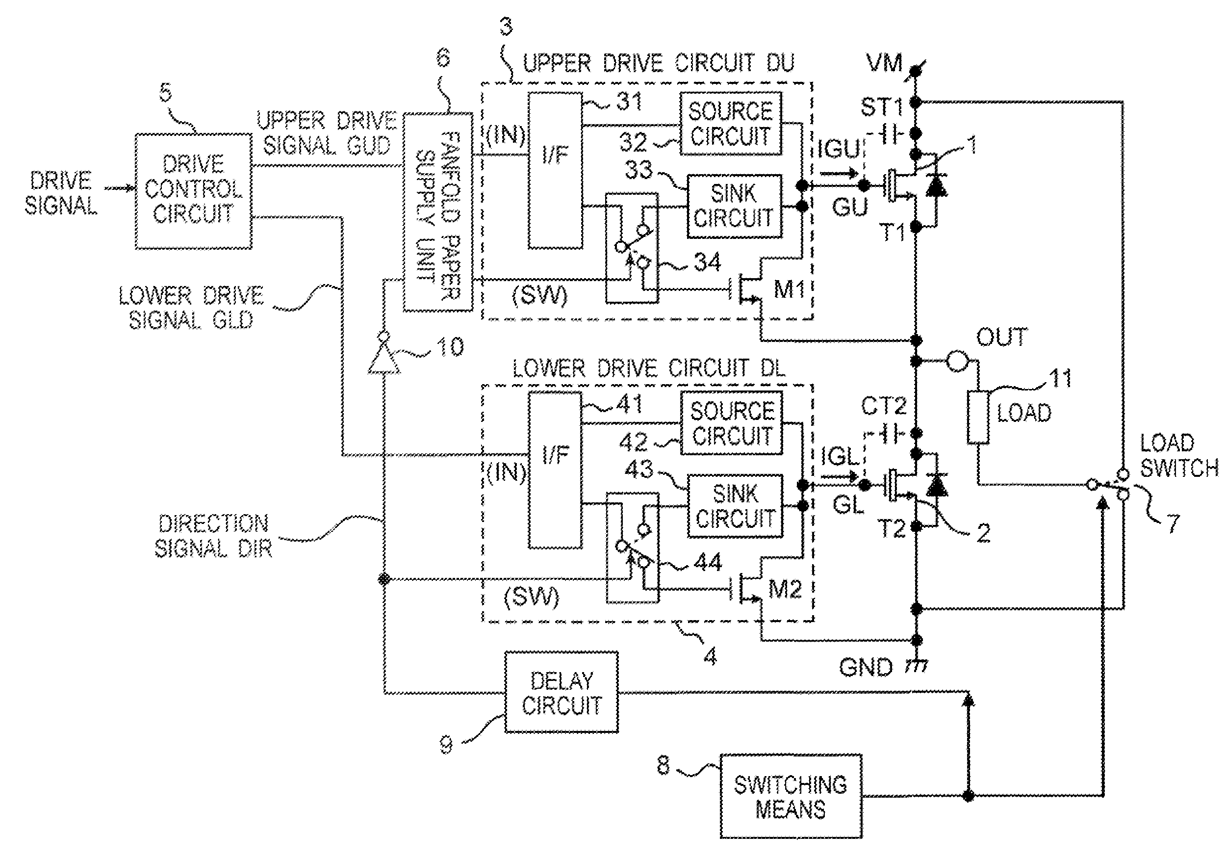
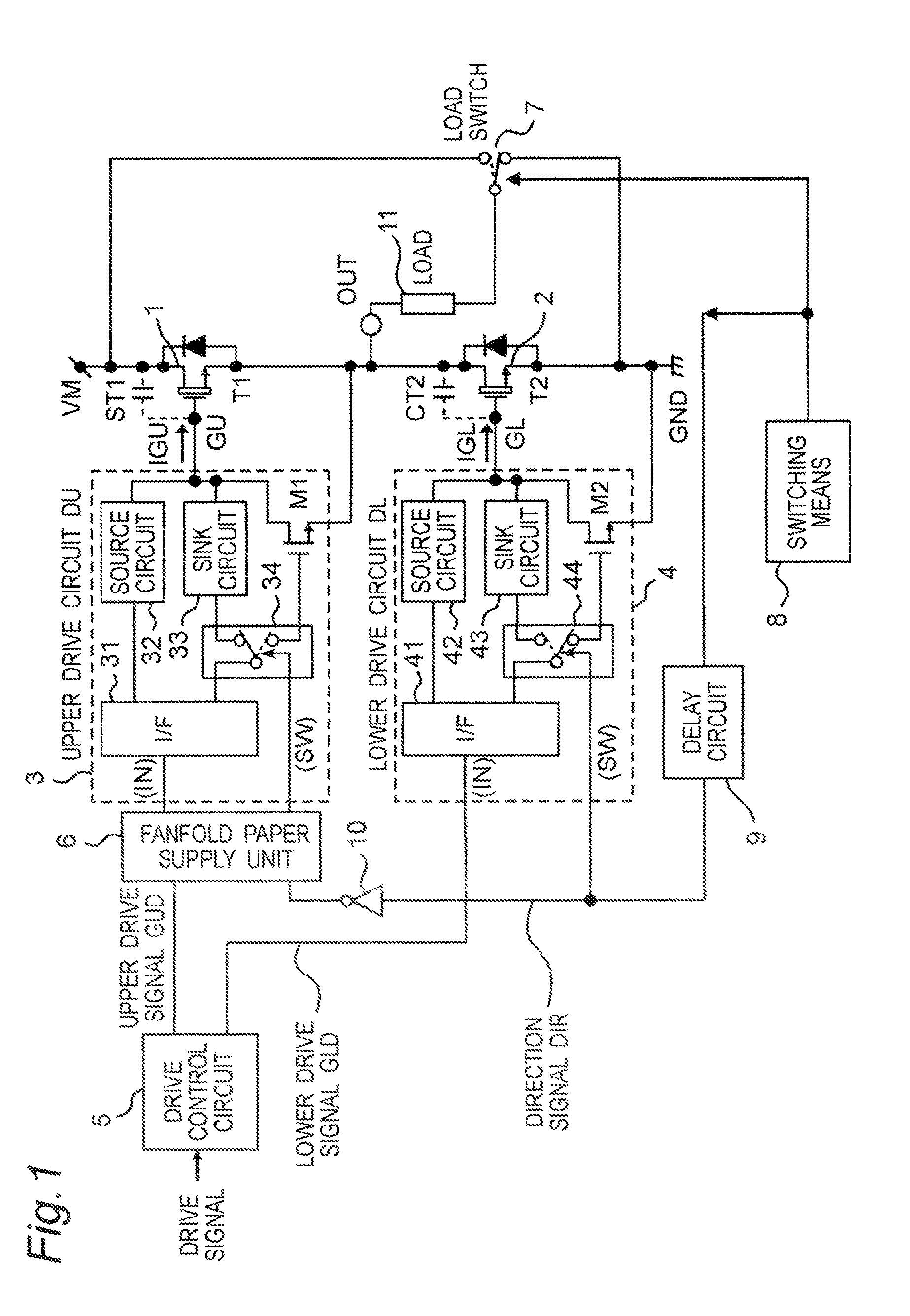
[0142]FIG. 1 describes the configuration of a drive device according to a preferred embodiment of the invention. A first embodiment of a half-bridge circuit as an example of a drive device according to the invention is described below with reference to FIG. 1.
[0143]FIG. 1 shows a half-bridge circuit using a drive circuit according to the first embodiment of the invention.
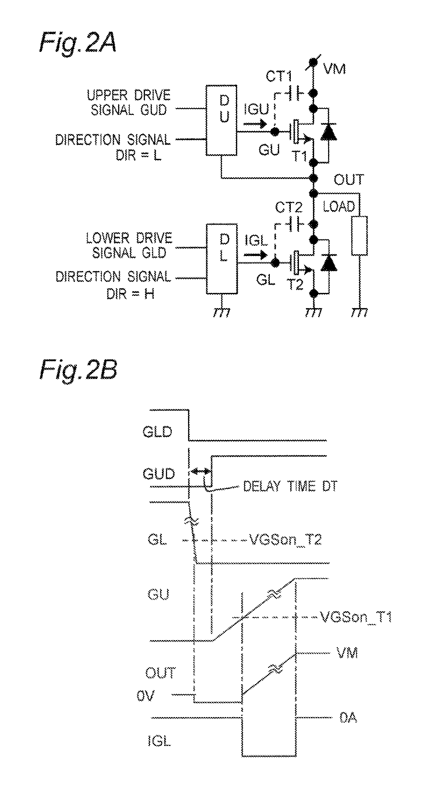
[0144]The half-bridge circuit includes: switching device T1 and switching device T2, which in this embodiment of the invention are two power MOSFET transistors to which a capacitive current flows to the control terminal, that is, the gate, thereof during the off period; an upper drive circuit DU and a lower drive circuit DL that respectively drive the transistors T1 and T2; a drive control circuit 5 that signal processes the drive signal that drives the half-bridge circuit, and generates an upper drive signal GUD that is input to the upper drive circuit DU that drives the upper transistor T1, and a lower drive signa...
embodiment 2
[0178]FIG. 9 shows the configuration of a second embodiment of the invention using the drive circuit according to the first embodiment and a drive direction detection circuit 100. The operation of the second embodiment is described below.
[0179]FIG. 9 shows a half-bridge circuit using the drive circuit according to the first embodiment and a drive direction detection circuit 100.
[0180]The half-bridge circuit includes: switching devices T1 and T2, which in this embodiment of the invention are two power MOSFET transistors to which a capacitive current flows to the control terminal, that is, the gate, thereof during the off period; an upper drive circuit DU and a lower drive circuit DL that respectively drive the transistors T1 and T2; a drive control circuit 5 that signal processes the drive signal that drives the half-bridge circuit, and generates an upper drive signal GUD that is input to the upper drive circuit DU that drives the upper transistor T1, and a lower drive signal GLD tha...
embodiment 3
[0203]FIG. 12 shows the configuration of a third embodiment of the invention using the drive circuit according to the first embodiment of the invention and a drive direction detection circuit 200 that is a modification of the drive direction detection circuit 100 in the second embodiment of the invention. The operation of this third embodiment is described below.
[0204]The third embodiment shown in FIG. 12 is a combination of the first embodiment and the second embodiment.
[0205]The difference with the second embodiment is the drive direction detection circuit 200 used in the third embodiment. This drive direction detection circuit 200 additionally has a differential pulse circuit 202 that receives output signals from the switching means 8 that controls the load switch 7 or a delay circuit 9 that is disposed according to the load conditions, and outputs direction signal DIR.
[0206]The differential pulse circuit 202 outputs set pulse S_EX and reset pulse R_EX having a particular pulse w...
PUM
 Abstract
Description
Claims
Application Information