Embedded printed circuit board and method of manufacturing the same

a printed circuit board and embedded technology, applied in the direction of chemistry apparatus and processes, semiconductor/solid-state device details, synthetic resin layered products, etc., can solve the problems of large cavity size, large machining time, and increased process costs

Inactive Publication Date: 2011-12-01
SAMSUNG ELECTRO MECHANICS CO LTD
View PDF9 Cites 27 Cited by
  • Summary
  • Abstract
  • Description
  • Claims
  • Application Information

AI Technical Summary

Problems solved by technology

However, the method using the mechanical drill, the punch, the laser drill, etc., does not form the cavity to accurately conform to the chip size due to a limitation in mechanical tolerance, thereby leading to a problem of forming the cavity larger than the chip and filling the remaining portion of the cavity.
In addition, in the

Method used


Image

  • Embedded printed circuit board and method of manufacturing the same
  • Embedded printed circuit board and method of manufacturing the same
  • Embedded printed circuit board and method of manufacturing the same

Examples


Embodiment Construction

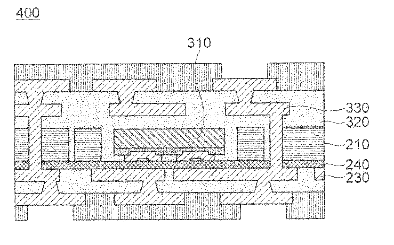
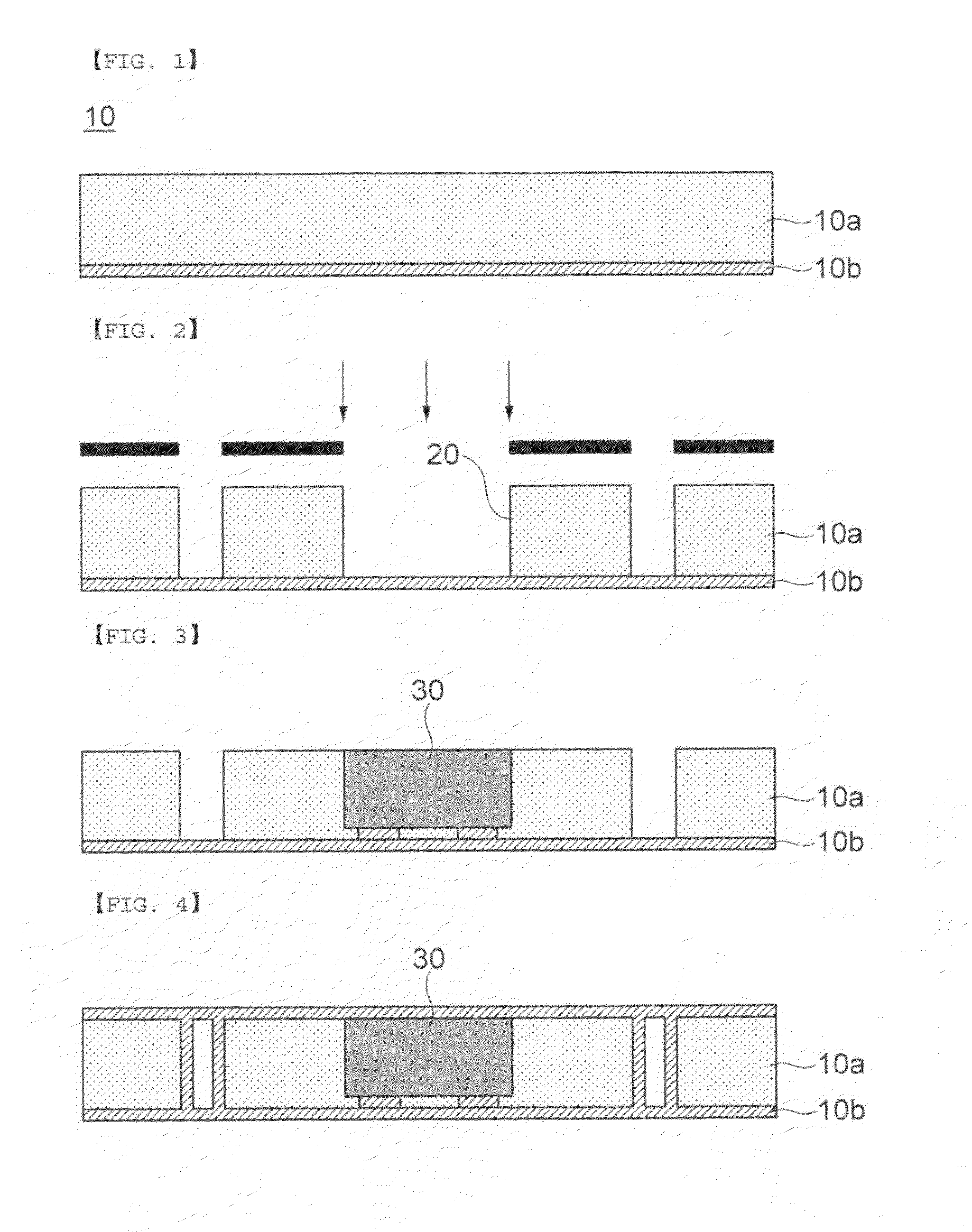
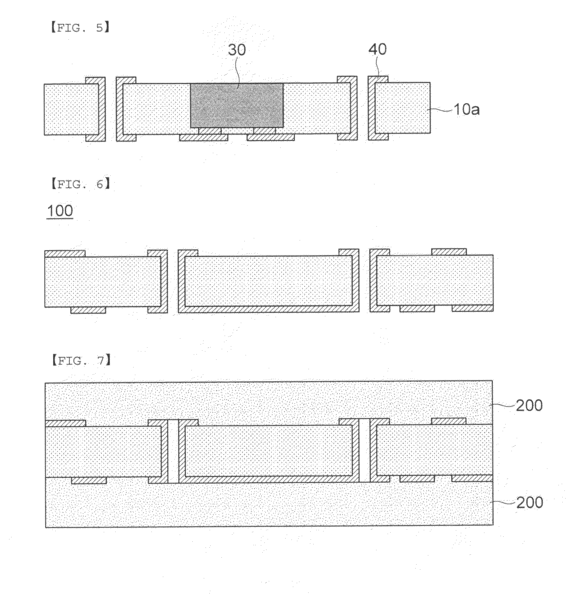
[0056]Hereinafter, an embedded printed circuit board according to exemplary embodiments of the present invention will be described in detail with reference to the accompanying drawings. The exemplary embodiments of the present invention to be described below are provided by way of example so that the idea of the present invention can be sufficiently transferred to those skilled in the art to which the present invention pertains. Therefore, the present invention may be modified in many different forms and it should not be limited to the embodiments set forth herein. In the drawings, the size, and the thickness of the device may be exaggerated for convenience. Like reference numerals denote like elements throughout the specification.

[0057]FIGS. 1 to 5 are cross-sectional views showing an embedded printed circuit board according to a first exemplary embodiment of the present invention.

[0058]Referring to FIGS. 1 to 5, an embedded printed circuit board according to the present invention ...


PUM

PropertyMeasurementUnit
Exposure limitaaaaaaaaaa
Photosensitivityaaaaaaaaaa
Degree of freedomaaaaaaaaaa

Abstract

Disclosed herein are an embedded printed circuit board and a method of manufacturing the same. The embedded printed circuit board includes: an insulating layer on which a cavity is formed; a chip mounted on the cavity; and a circuit layer formed on the insulating layer, wherein the insulating layer is made of photosensitive compositions including photosensitive monomer and photoinitiator. As a result, the cavity can be formed by selectively using only the insulating layer, thereby making it possible to secure a degree of freedom in the design of the embedded printed circuit board.

Description

CROSS REFERENCE TO RELATED APPLICATION[0001]This application claims the benefit under 35 U.S.C. Section 119 of Korean Patent Application Nos. 10-2010-0048647, filed on May 25, 2010 and 10-2010-0089951, filed on Sep. 14, 2010, entitled “Embedded Printed Circuit Board And Method Of Manufacturing The Same”, which is hereby incorporated by reference in its entirety into this application.BACKGROUND OF THE INVENTION[0002]1. Technical Field[0003]The present invention relates to an embedded printed circuit board and a method of manufacturing the same, and more particularly, to an embedded printed circuit board and a method of manufacturing the same capable of forming a cavity for embedding a chip on a photosensitive film by an exposure and development process.[0004]2. Description of the Related Art[0005]With the development of the electronic industry, a demand for high-functional and small-sized electronic parts is increasing. In particular, a printed circuit board is getting slimmer in ord...

Claims


Application Information

Patent Timeline
IPC IPC(8): H05K1/03B32B38/00H05K1/02B32B38/10H05K3/30B32B37/02B32B38/08
CPCH01L23/13Y10T29/4913H01L23/49822H01L21/4846H01L23/5389H05K1/0353H05K1/185H05K1/188H05K3/0023H05K3/4676H05K2201/10674H05K2203/1469H01L23/49827H01L24/18H01L2224/04105H01L2224/2518H01L2224/32245H01L2224/73267H01L2224/92244H05K1/0306H05K1/183H05K3/30H05K2201/0137H05K2201/0209H01L23/145H01L2924/12042H01L2224/83192H01L24/19H01L2924/00
Inventor JUNG, HYUNGMICHO, JAECHOONLEE, CHOONKEUNJEONG, TAESUNGLEE, SEUNGEUNPARK, JINSUNSHIN, YEENA
Owner SAMSUNG ELECTRO MECHANICS CO LTD
Why Eureka
Try Eureka