Programming method and device for a buffer cache in a solid-state disk system

a solid-state disk and buffer cache technology, applied in the direction of memory adressing/allocation/relocation, instruments, input/output to record carriers, etc., can solve the problems of small power consumption, non-volatile memory that takes a relatively short read/write time, etc., to improve writing performance and reduce delay

Active Publication Date: 2011-12-01
KIOXIA CORP
View PDF7 Cites 42 Cited by
  • Summary
  • Abstract
  • Description
  • Claims
  • Application Information

AI Technical Summary

Benefits of technology

[0016]According to embodiments of the present invention, a method and apparatus for programming a buffer cache in a Solid State Disk (SSD) system that may include a buffer cache unit to store pages, a memory unit including a plurality of memory chips, and a control unit to select at least one of the pages as a victim page, based on a delay occurring when a page is stored in at least one target memory chip among the plurality of memory chips, and that may improve a writing performance by reducing a delay occurring when storing a page of a buffer cache.

Problems solved by technology

Recently, a non-volatile memory that takes a relatively short read / write time, consumes a small amount of power, and occupies a small amount of space, compared with a magnetic disk, is rapidly replacing the magnetic disk.
However, if the flash chip storing the original page is performing a writing operation, the controller is required to delay reading of the original page until the writing operation is terminated.

Method used


Image

  • Programming method and device for a buffer cache in a solid-state disk system
  • Programming method and device for a buffer cache in a solid-state disk system
  • Programming method and device for a buffer cache in a solid-state disk system

Examples


Embodiment Construction

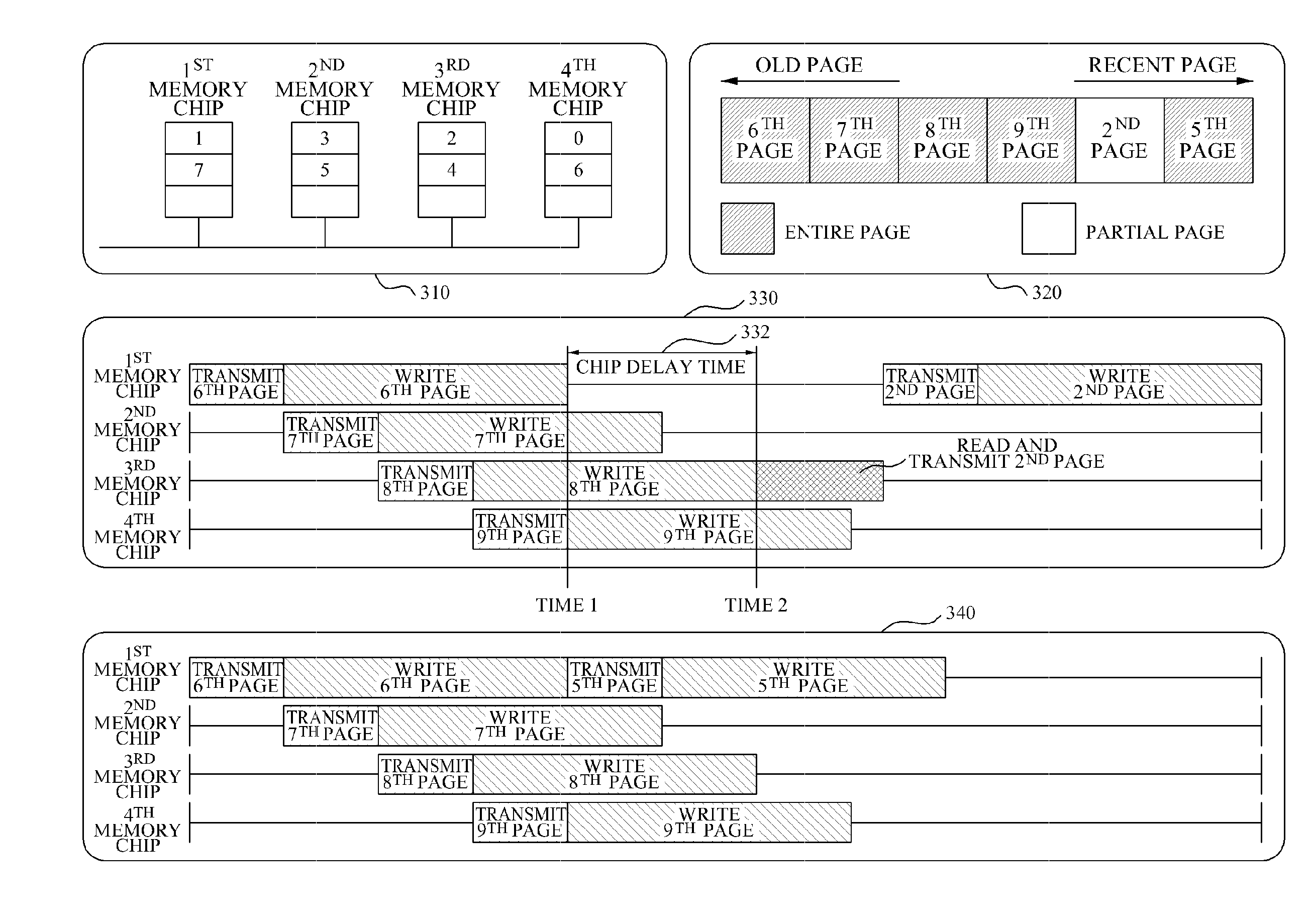
[0021]Reference will now be made in detail to embodiments of the present invention, examples of which are illustrated in the accompanying drawings, wherein like reference numerals refer to the like elements throughout. The embodiments are described below in order to explain the present invention by referring to the figures.

[0022]Embodiments of the present invention relate to a programming method and apparatus that may reduce a delay occurring when a page of a buffer cache is stored in a memory including a plurality of memory chips, in a Solid State Disk (SSD) system. A configuration of the SSD system will be described hereinafter with reference to FIG. 1.

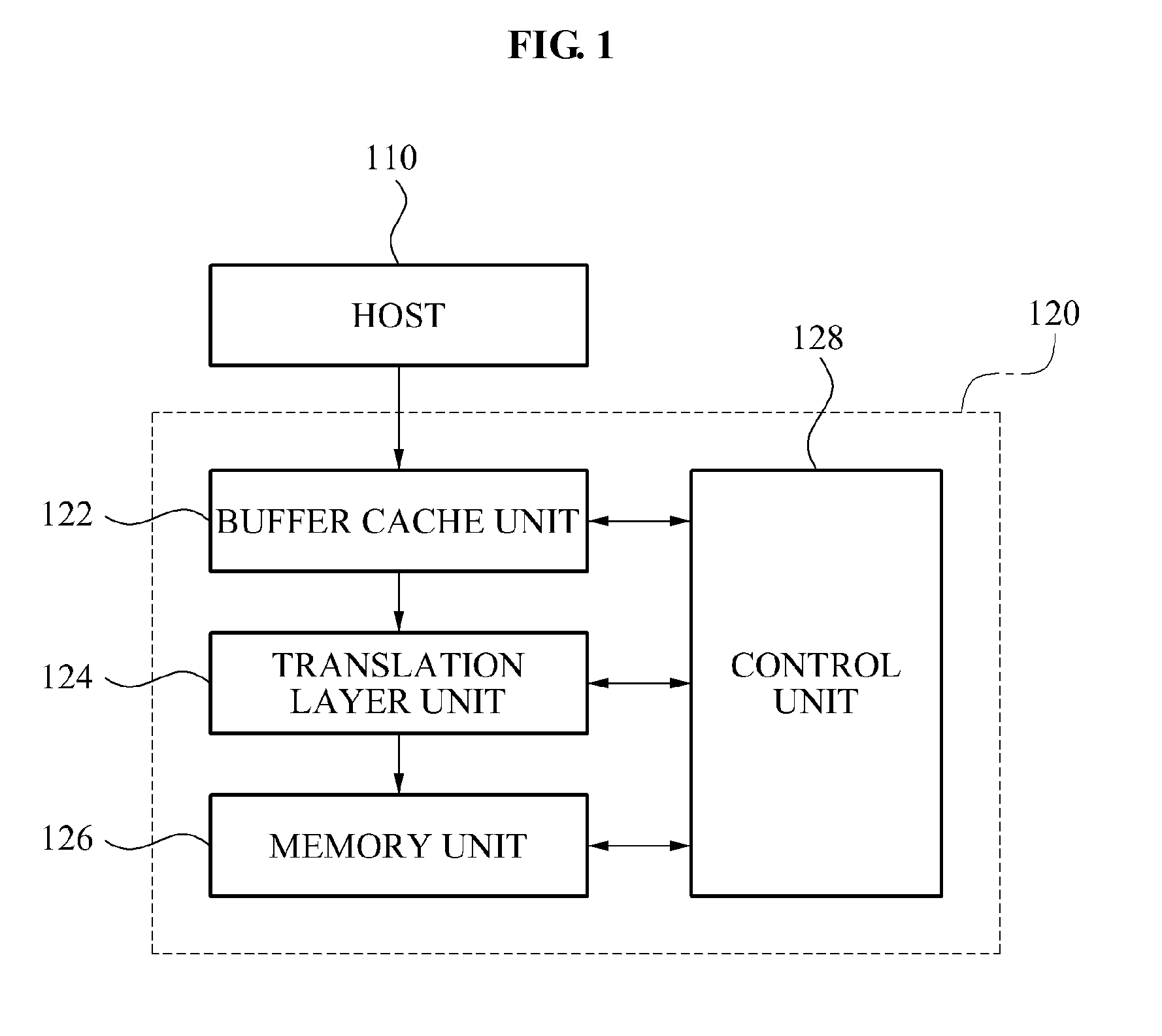
[0023]FIG. 1 is a block diagram illustrating a configuration of an SSD system 120 that may store a page of a buffer cache without a delay according to an embodiment of the present invention.

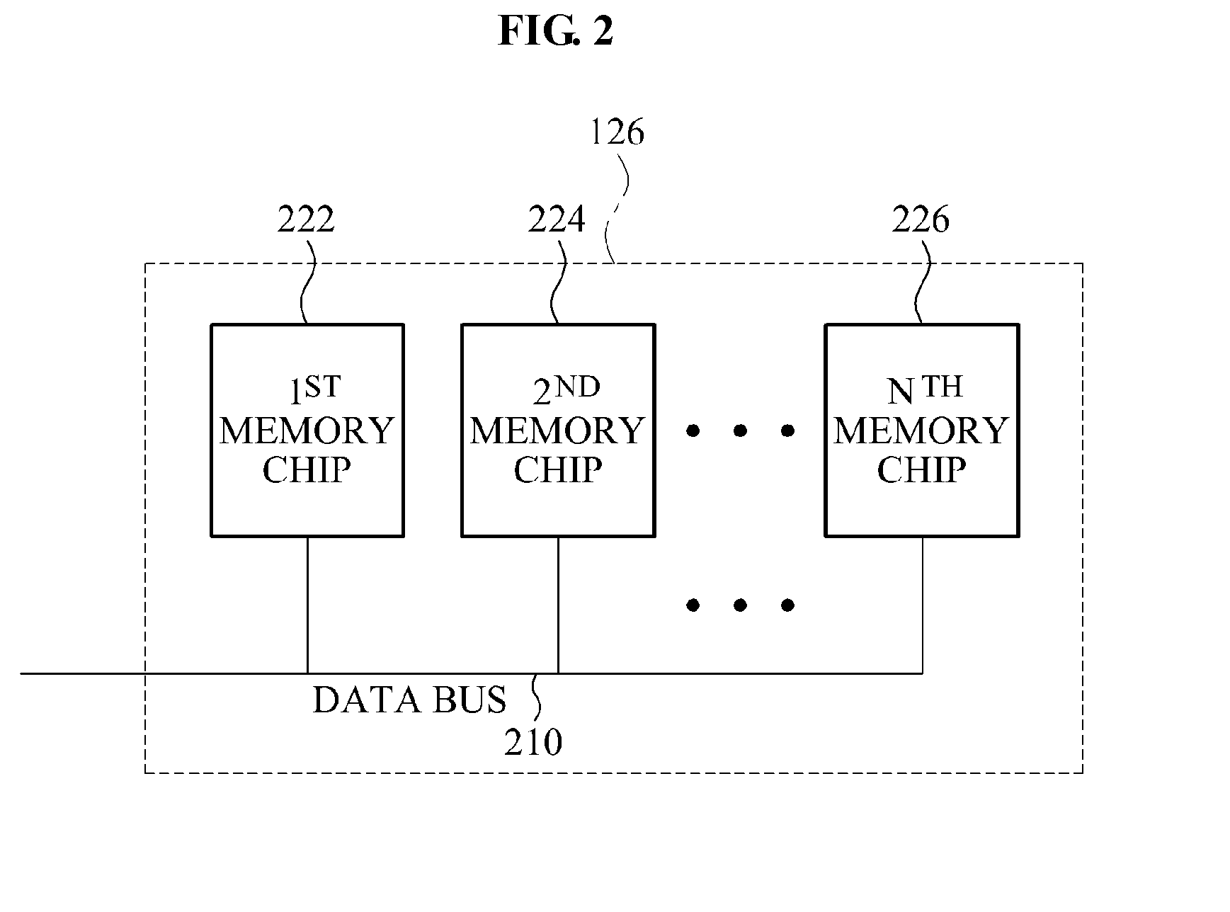
[0024]Referring to FIG. 1, the SSD system 120 may include a buffer cache unit 122, a translation layer unit 124, a memory unit 126, and a contro...


PUM


Abstract

Provided are a method and apparatus for programming a buffer cache in a Solid State Disk (SSD) system. The buffer cache programming apparatus in the SSD system may include a buffer cache unit to store pages, a memory unit including a plurality of memory chips, and a control unit to select at least one of the page as a victim page, based on a delay occurring when a page is stored in at least one target memory chip among the plurality of memory chips.

Description

TECHNICAL FIELD[0001]The present invention relates to a method and apparatus for programming a buffer cache in a Solid State Disk (SSD) system, and more particularly, to a programming method and apparatus that may reduce a delay occurring when a page of a buffer cache is stored in a memory including a plurality of memory chips, in an SSD system.BACKGROUND ART[0002]A storage device for storing data may include, for example, a magnetic disk, a semiconductor memory, and the like. Since physical characteristics are different for each type of storage device, a management method corresponding to the distinctive physical characteristics is required.[0003]Conventionally, magnetic disks are widely used as storage devices. A read / write time of the magnetic disk takes an average of several milliseconds per kilobyte. Additionally, since an arrival time of an arm of the magnetic disk is different, depending on a physical location that stores data, the read / write time of the magnetic disk varies....

Claims


Application Information

Patent Timeline
Patent Type & Authority Applications(United States)
IPC IPC(8): G06F12/00
CPCG06F12/0246G06F2212/214G06F12/121G06F12/0866G06F3/06G06F12/02G06F12/16G06F13/10
Inventor SEOL, JIN-HOMAENG, SEUNG-RYOULKIM, JIN-SOOKIM, JAE-GEUKSHIM, HYO-TAEKPARK, HAN-MOOK
Owner KIOXIA CORP
Why Eureka
Try Eureka