Impedance Adjustment Circuit for Adjusting Planar Antennas

a planar antenna and impedance adjustment technology, applied in the direction of resonant antennas, substantially flat resonant elements, independent non-interacting antenna combinations, etc., can solve the problems of large number of circuit elements, so as to reduce complexity, reduce the effect of tuning range and reduced number of circuit elements

Active Publication Date: 2011-12-08
QUALCOMM TECHNOLOGIES INC
View PDF5 Cites 12 Cited by
  • Summary
  • Abstract
  • Description
  • Claims
  • Application Information

AI Technical Summary

Benefits of technology

[0006]In one aspect, the present invention specifies an impedance matching circuit with reduced comp

Problems solved by technology

One problem of known impedance matching circuits for planar antennas lies in the fact that either the tuning range is too small or the impedance mat

Method used


Image

  • Impedance Adjustment Circuit for Adjusting Planar Antennas
  • Impedance Adjustment Circuit for Adjusting Planar Antennas
  • Impedance Adjustment Circuit for Adjusting Planar Antennas

Examples


Embodiment Construction

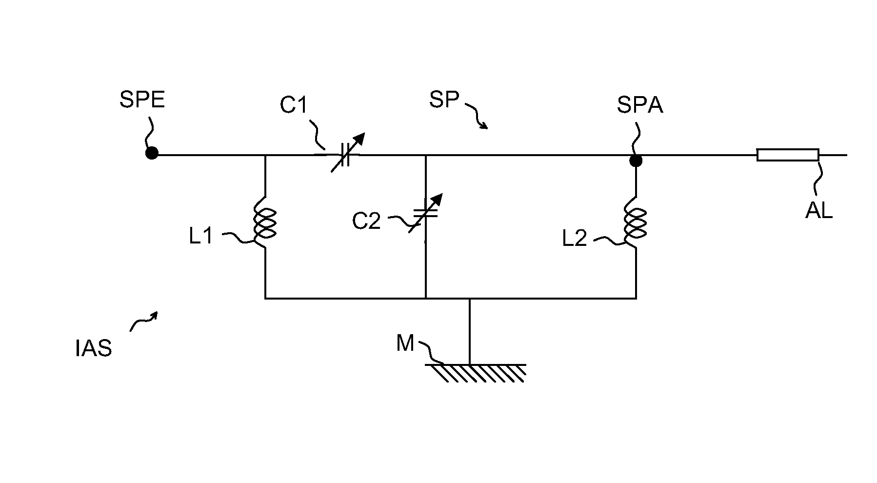
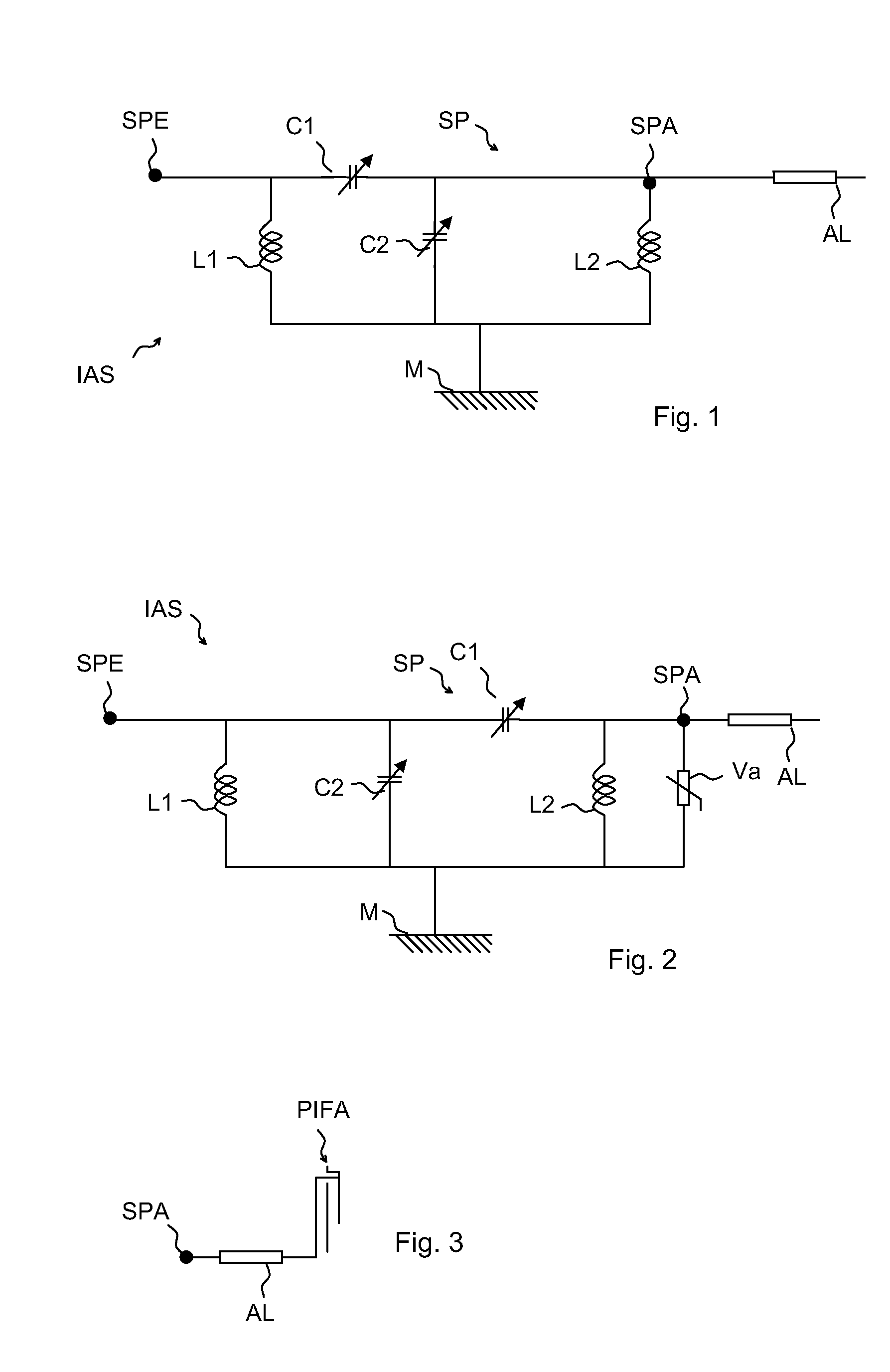
[0033]FIG. 1 shows an impedance matching circuit IAS for planar antennas, which has low complexity and enables a sufficient tuning range. A variable capacitive element C1 is connected in signal path SP with signal path input SPE and signal path output SPA. In addition, there is an inductive element L1 connected between the signal path input SPE and ground M. In addition, a variable capacitive element C2 and an inductive element L2 are connected between the signal path output SPA and ground M. Further, the signal path output SPA is connected to an antenna line AL.

[0034]FIG. 2 shows an alternative embodiment of the impedance matching circuit IAS, in which, in contrast to FIG. 1, the second variable capacitive element C2 is connected between the signal path input SPE and ground M. In addition, a variable resistive element VA is connected between the signal path output SPA and ground M.

[0035]Both the first inductive element L1 and the second inductive element L2 are, in addition to thei...


PUM


Abstract

An impedance matching circuit for matching planar antennas includes a signal path with a signal path input and a signal path output. A first capacitive element with variable capacitance is connected between the signal path input and signal path output. A second capacitive element with variable capacitance is connected between the signal path and ground. A first inductive element is connected between the signal path input and ground. A second inductive element is connected between the signal path output and ground. An antenna line with an impedance between 30 and 60 ohm is connected to the signal path output.

Description

[0001]This patent application is a national phase filing under section 371 of PCT / EP2009 / 068010, filed Dec. 29, 2009, which claims the priority of German patent application 10 2009 004 720.4, filed Jan. 15, 2009, each of which is incorporated herein by reference in its entirety.TECHNICAL FIELD[0002]The invention concerns an impedance matching circuit to match the impedance of planar antennas of the PIFA type (Planar Inverted F Antenna).BACKGROUND[0003]Planar antennas are antennas that are not adjusted to a specific impedance, but rather require a matching circuit for maximum power transmission. Matching is necessary if the power loss in signal transmission to a non-impedance-matched antenna is to be reduced. Planar antennas, as are used in mobile communications equipment, react by a change of their impedance to changed external effects or proximity to objects such as hands or other body parts of a user, or even metal surfaces.[0004]Connecting a planar antenna to an associated impeda...

Claims


Application Information

Patent Timeline
IPC IPC(8): H01Q1/50
CPCH01Q9/0407H01Q21/28H04B1/18H04B1/0458H03H7/38
Inventor SCHMIDHAMMER, EDGAR
Owner QUALCOMM TECHNOLOGIES INC
Why Eureka
Try Eureka