MOS transistor structure with easy access to all nodes

Active Publication Date: 2011-12-29
DIALOG SEMICONDUCTOR
View PDF3 Cites 22 Cited by
  • Summary
  • Abstract
  • Description
  • Claims
  • Application Information

AI Technical Summary

Benefits of technology

[0007]In accordance with the objects of this invention, a transistor device structured such that the bulk, gate, drain, and source are all accessible from all four edges of the device is provided. The transistor is created with a four-metal CMOS process. A bulk connection can be made with Metal1, which is all around the device. A gate connection can be made with Metal2, which is all around the device. Additionally, a drain/source connection can be made with Metal3, which is all aro

Problems solved by technology

Unfortunately the current distribution insid

Method used


Image

  • MOS transistor structure with easy access to all nodes
  • MOS transistor structure with easy access to all nodes
  • MOS transistor structure with easy access to all nodes

Examples


Embodiment Construction

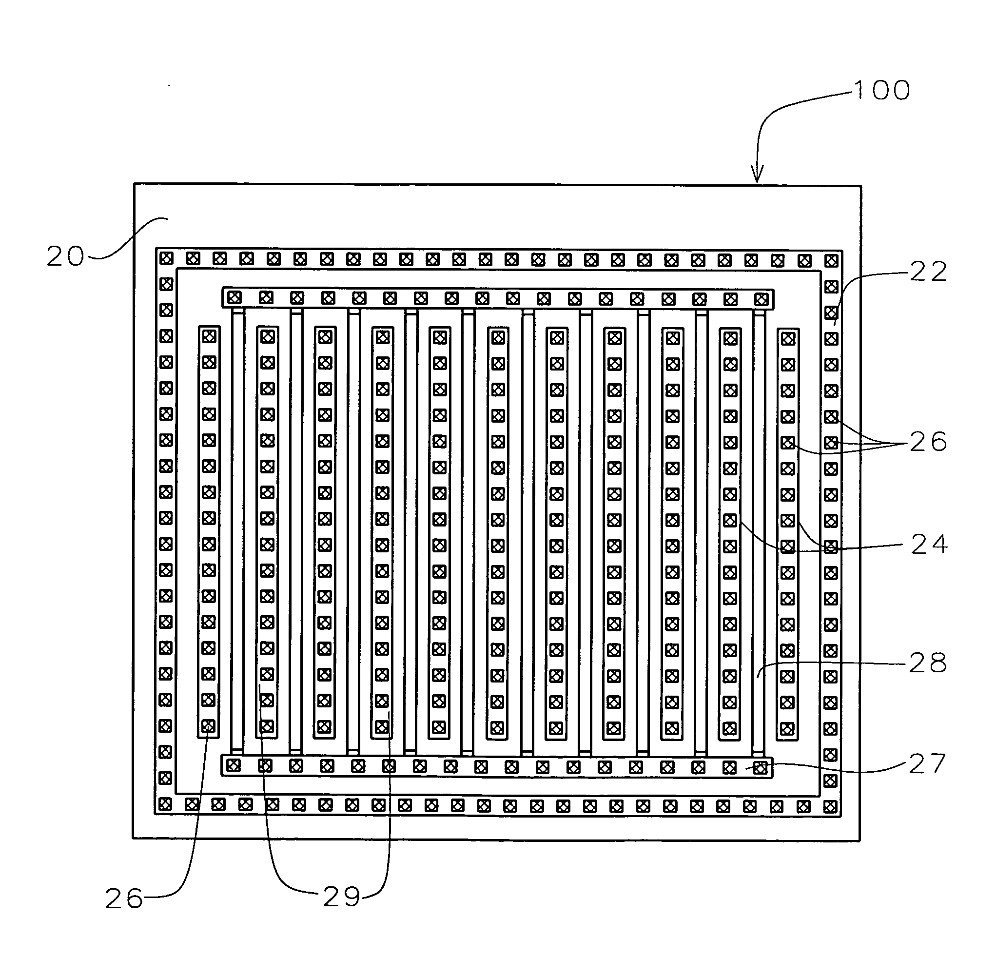
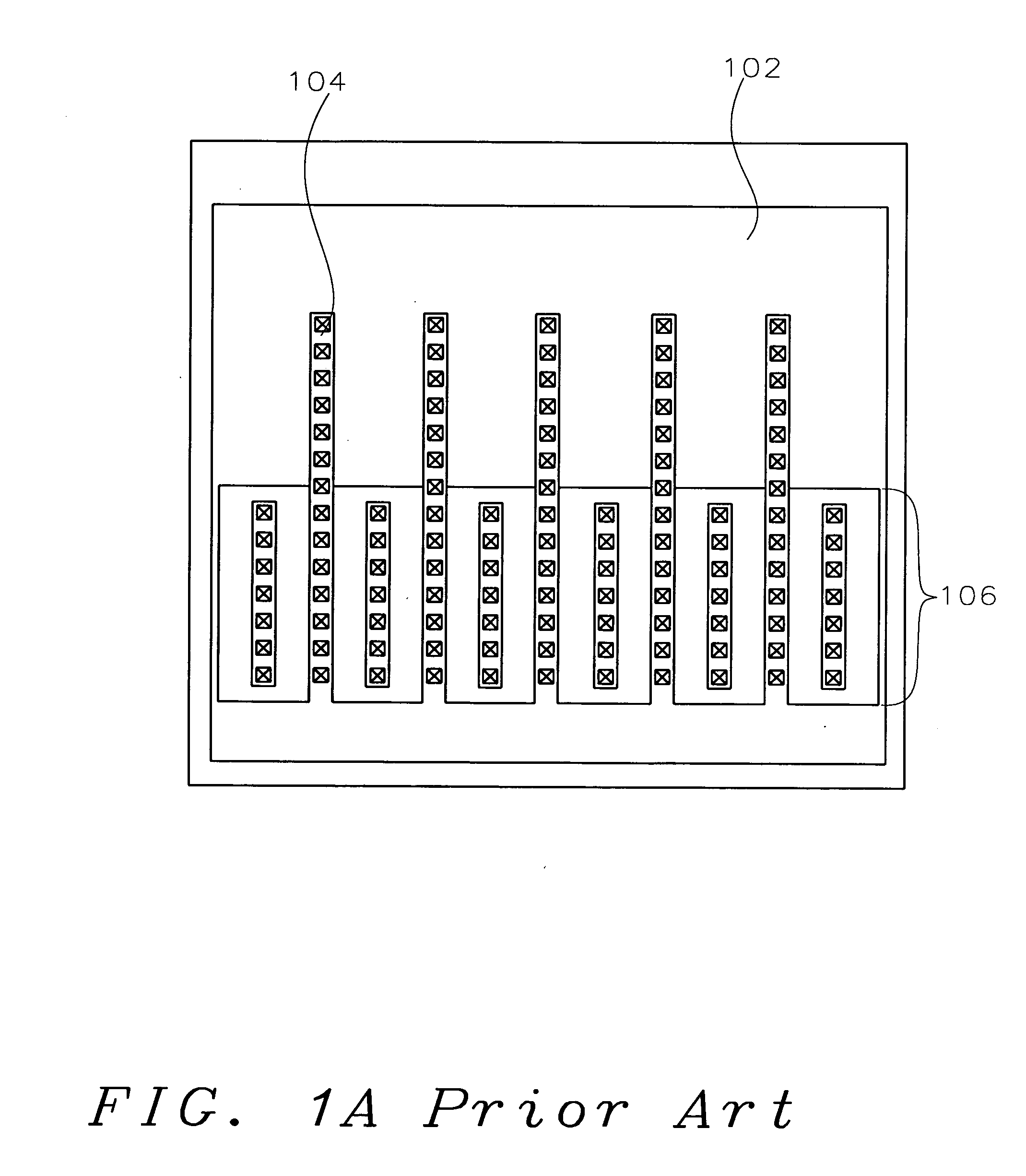
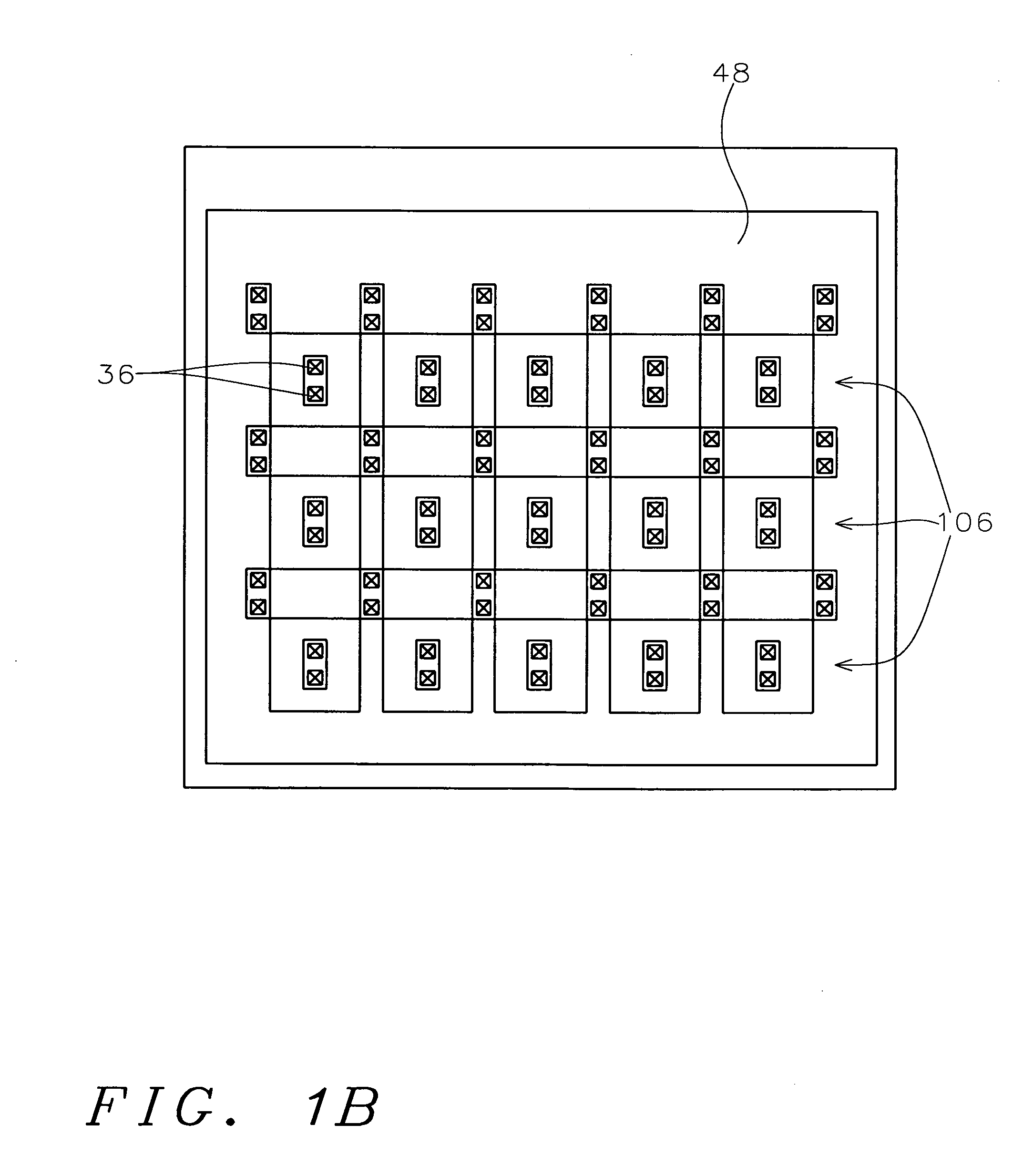
[0019]Briefly reviewing the invention in U.S. Pat. No. 7,355,217, a transistor device is structured such that the bulk, gate, drain, and source are all accessible from all four edges of a rectangular device. The transistor is created with a four-metal CMOS process. A bulk connection can be made with Metal1, which is all around the device. A gate connection can be made with Metal2, which is all around the device. Additionally, a drain / source connection can be made with Metal3, which is all around the device. A source / drain connection can be made with Metal4, which is all around the device. The transistor structure may be used to create an array of transistors for a high power output stage, for example, with the transistors arranged in a checkerboard pattern. The connections of each transistor are automatic by abutting edges of the transistors.

[0020]The connection to the source / drain is by via stripes which are connected to less than half of the source / drain connection length of the s...


PUM


Abstract

A transistor device structured such that the bulk, gate, drain, and source are all accessible from all four edges of the device and such that current distribution is uniform over the device is provided. The transistor is created with a four-metal CMOS process. A bulk connection can be made with Metal 1, which is all around the device. A gate connection can be made with Metal 2, which is all around the device. Additionally, a drain/source connection can be made with Metal 3, which is all around the device. A source/drain connection can be made with Metal 4, which is all around the device. Source/drain connections are made with two or more evenly distributed via stripes to connect the source/drain parts of the transistor fingers. The transistor structure may be used to create an array of transistors for a high power output stage, with the transistors arranged in a checkerboard pattern. The connections of each transistor are automatic by abutting edges of the transistors.

Description

BACKGROUND OF THE INVENTION[0001](1) Field of the Invention[0002]The invention relates to transistors, and more particularly, to a structure suitable for high current transistor devices including an array of output transistors in which the source, drain, gate, and bulk of each of the output transistors in the array is accessible from all four edges of the transistor and in which good current distribution is achieved.[0003](2) Description of the Related Art[0004]Related U.S. Pat. No. 7,355,217, invented by the same inventor as the current invention and assigned to the same assignee, is hereby incorporated by reference in its entirety. The transistor structure of the referenced patent may be used to create large arrays of high current transistor devices very quickly in terms of the connections between the nodes of a big transistor device because all the connections between bulk, gate, drain and source are done automatically by only abutting the transistor cells. Unfortunately the curr...

Claims


Application Information

Patent Timeline
IPC IPC(8): H01L27/092H01L27/088
CPCH01L29/41758H01L29/78H01L29/4238
Inventor BRAND, JOERG
Owner DIALOG SEMICONDUCTOR
Why Eureka
Try Eureka