Driving device for semiconductor element

Active Publication Date: 2011-12-29
FUJI ELECTRIC CO LTD
View PDF3 Cites 27 Cited by
  • Summary
  • Abstract
  • Description
  • Claims
  • Application Information

AI Technical Summary

Benefits of technology

[0015]Since this alarm signal is a pulse sequence signal having a different pulse width for each of the plurality of protection circuits, measurement of the pulse width of the alarm signal by an external device makes it possible to recognize the protection circuit that has detected the protection operation state. Because the pulse sequence signal from the pulse signal generation circuit has the pulse width corresponding to the protection circuit that has first detected a need for a protection operation, mixture of pulse sequence signals is inhibited and erroneous detection in the external control device is avoided without failure.
[0024]In a driving device for a semiconductor element according to the invention, the driving device for driving each of the semiconductor elements composing a power conversion apparatus has a plurality of protection circuits for detecting information necessary for protection operation for the semiconductor element, and a pulse sequence signal having a pulse width different for each of the plurality of protection circuits is inhibited to output simultaneously. Therefore, the present invention has an effect that the protection circuits are accurately discriminated by the pulse width of the pulse sequence signal and erroneous detection of a protection operation state is avoided.
[0025]By mutually connecting every alarm terminal of the driving devices for a plurality of semiconductor elements composing the lower arm of the power convertor apparatus, when a state necessary for protection operation is detected in a driving device for a semiconductor element and an alarm signal is outputted, any alarm signal from the other driving devices for a semiconductor element is inhibited to output, thereby avoiding overlapping of alarm signals between the driving devices for a semiconductor element.

Problems solved by technology

As a result, if an alarm signal is outputted from any other alarm means simultaneously with the alarm means in operation or before the alarm signal of the alarm means in operation returns to ON state, an alarm signal is erroneously detected.
That is one of unsolved problems.
The conventional example disclosed in Patent Document 2 needs to output two types of signals of an alarm signal and an abnormality factor discriminating signal, which results in a complicated structure of a signal forming circuit.
That is another unsolved problem.
This protection circuit cannot make discrimination between collector current abnormality and chip temperature abnormality, but only determines that the IGBT is in a condition where an abnormality has been generated or there exist a sign of generating an abnormality.
Thus, the device of Patent Document 3 cannot make discrimination among abnormality factors.
That is another largely unsolved problem.

Method used


Image

  • Driving device for semiconductor element
  • Driving device for semiconductor element
  • Driving device for semiconductor element

Examples


Embodiment Construction

[0030]Some aspects of preferred embodiments will be described in the following with reference to the accompanying drawings.

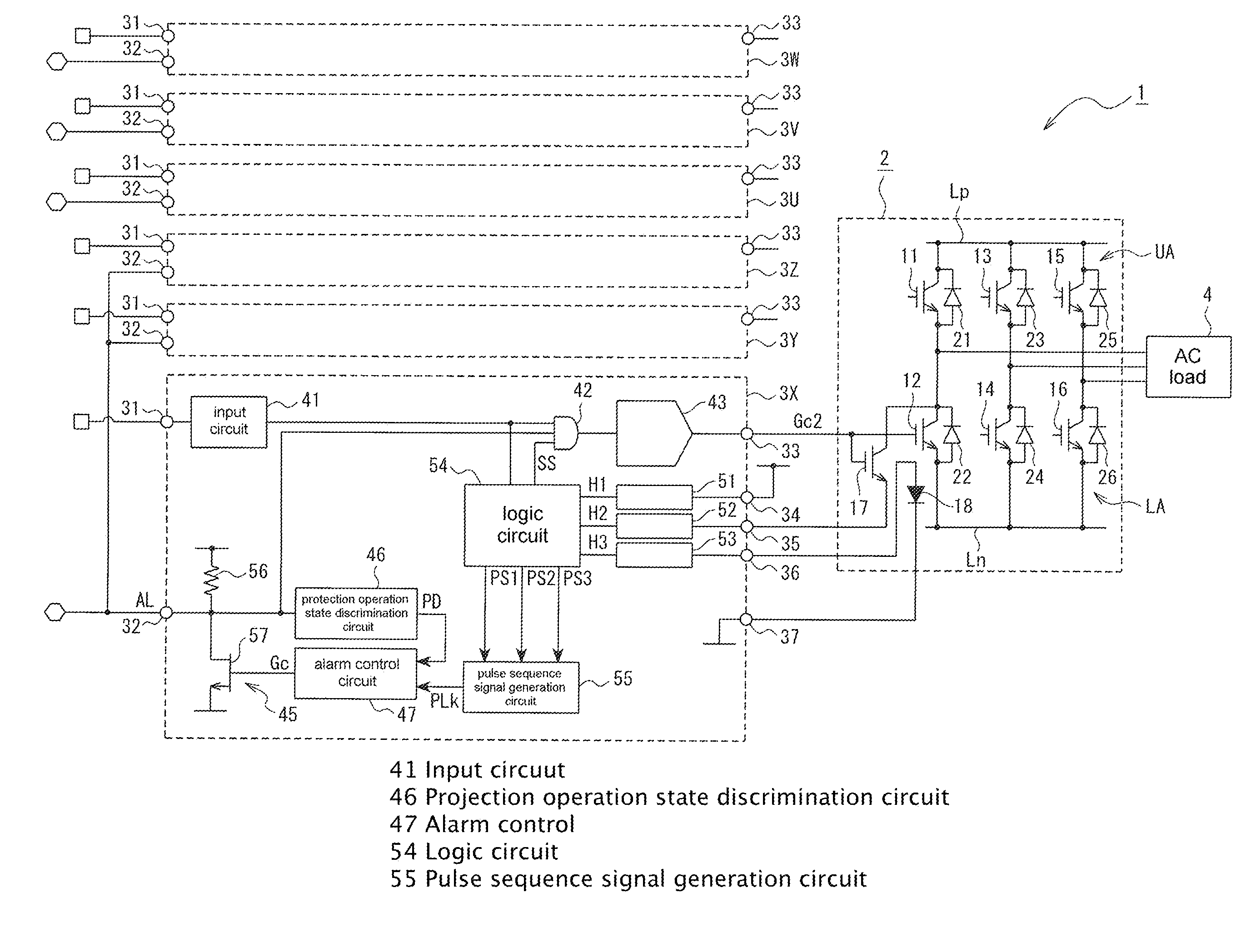
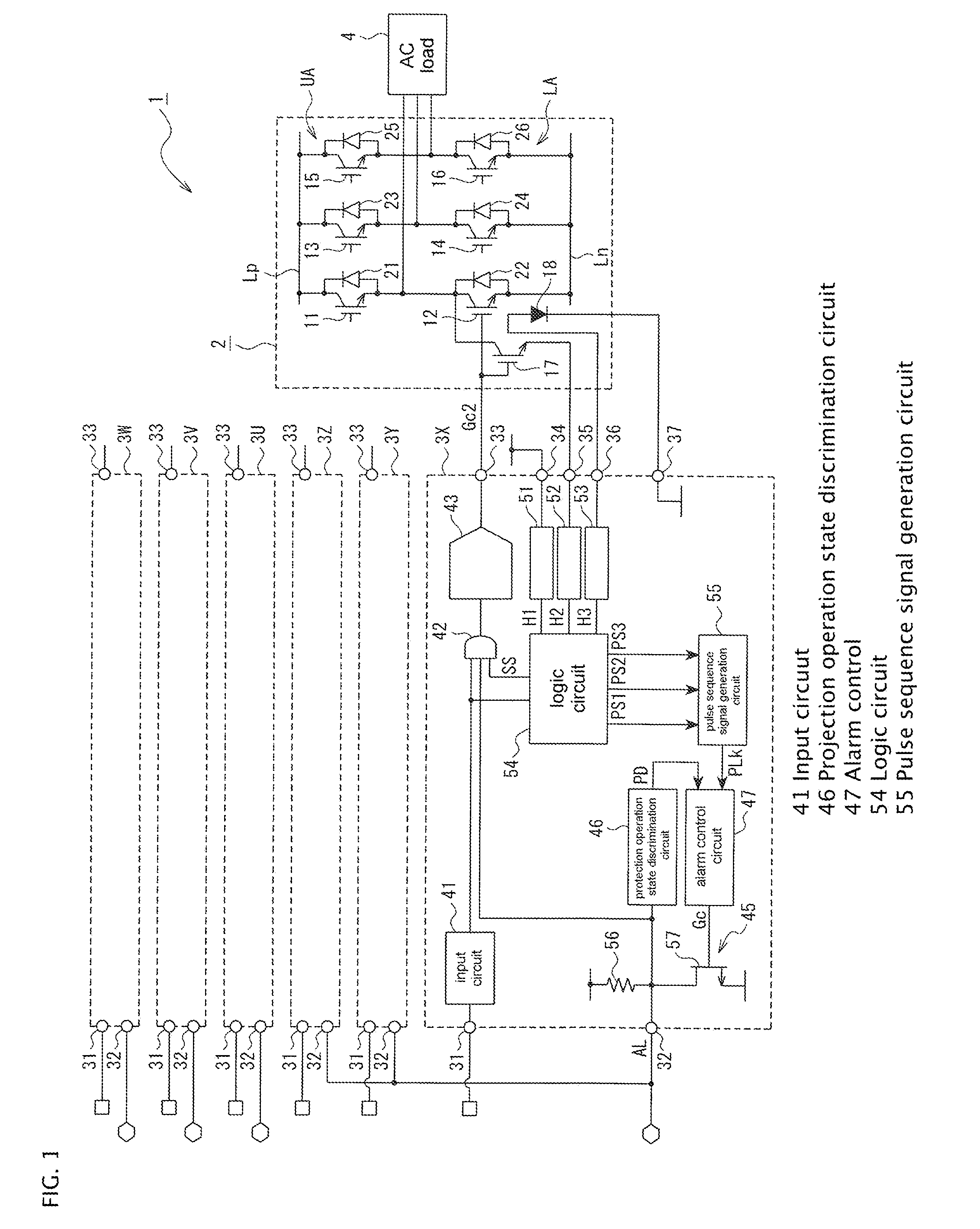
[0031]FIG. 1 is a block diagram of a power conversion apparatus to which a driving device for a semiconductor element of an embodiment according to the present invention is applied. Referring to FIG. 1, the power conversion apparatus 1 comprises an inverter 2 that converts DC power to AC power and driver ICs 3U through 3Z for phases, which are driving devices for semiconductor elements for individually driving semiconductor elements for the phases composing the inverter 2.

[0032]The inverter 2 has six IGBTs (insulated gate bipolar transistors) 11 through 16, which are semiconductor elements. A series-connected circuit of IGBTs 11 and 12, a series-connected circuit of IGBTs 13 and 14, and a series-connected circuit of IGBTs 15 and 16 are connected between a positive line Lp and a negative line Ln that are connected to a DC power supply and supplied with DC power, ...


PUM


Abstract

A driving device for driving a semiconductor element can include a plurality of protection circuits that detect information necessary for performing protection operation for semiconductor elements that include a power conversion apparatus, a pulse signal generation circuit that sets a pulse sequence signal with a pulse width differently for each of the protection circuits and outputs a pulse sequence signal corresponding to the protection circuit that has been first detected a need for protection operation. The device can also include an alarm signal forming circuit that forms an alarm signal by ON-OFF control of a switching element and externally outputs the alarm signal, and a protection operation state discrimination circuit that discriminates existence of a protection operation state based on the alarm signal from the alarm signal forming circuit, and an alarm control circuit that delivers the pulse sequence signal outputted from the pulse signal generation circuit.

Description

BACKGROUND OF THE INVENTION[0001]1. Field of the Invention[0002]Embodiments of the present invention relate to a driving device for a semiconductor element that drives a semiconductor element composing a power conversion apparatus, for example, and has a protection operation discriminating function.[0003]2. Description of the Related Art[0004]A related type of driving device for a semiconductor element is disclosed in Japanese Unexamined Patent Application Publication No. H08-070580 (also referred to herein as “Patent Document 1”), for example. The driving device comprises an alarm circuit that is provided for an intelligent power module (IPM) that is a power transistor module for driving an inverter, and comprises an overcurrent alarm means, an overvoltage alarm means, and an overheat alarm means.[0005]In the conventional example disclosed in Patent Document 1, the overcurrent alarm means outputs a first alarm signal having a first pulse width upon detection of an overcurrent state...

Claims


Application Information

Patent Timeline
IPC IPC(8): H02H7/00
CPCH02H7/122
Inventor MOTOHASHI, SATORUNAKAMORI, AKIRA
Owner FUJI ELECTRIC CO LTD
Why Eureka
Try Eureka