Microelectromechanical system (MEMS) carrier and method of fabricating the same

a microelectromechanical system and carrier technology, applied in the field of carriers, can solve the problems of increasing the height of the overall structure and the miniaturization of electronic products, and achieve the effects of reducing the height, reducing the path of signal received by the mems, and reducing the heigh

Inactive Publication Date: 2012-02-09
UNIMICRON TECH CORP
View PDF5 Cites 1 Cited by
  • Summary
  • Abstract
  • Description
  • Claims
  • Application Information

AI Technical Summary

Benefits of technology

[0022]Accordingly, the MEMS carrier of the present invention and method of fabricating the same, through the formation of the patterned metal layer on the carrier layer, an MEMS and ASIC are allowed to be mounted on the patterned metal layer and the carrier layer. As compared with the prior art, there is no need in the present invention to use a circuit board. Therefore, the overall structure has a reduced height, and is more advantageous in the miniaturization of electronic products.
[0023]Furthermore, since the MEMS is allocated on the patterned metal layer, the acoustic hole is thus located under the MEMS. As a result, a path of signal received by the MEMS is shortened, and the signal stability and transmission speed are enhanced.

Problems solved by technology

Accordingly, the overall structure has an increased height, which is disadvantageous in miniaturization of electronic products.
Hence, how to overcome the drawbacks of the prior art is becoming one of the critical issues in the art.

Method used


Image

  • Microelectromechanical system (MEMS) carrier and method of fabricating the same
  • Microelectromechanical system (MEMS) carrier and method of fabricating the same
  • Microelectromechanical system (MEMS) carrier and method of fabricating the same

Examples


Embodiment Construction

[0031]The following illustrative embodiments are provided to illustrate the disclosure of the present invention; those in the art can apparently understand these and other advantages and effects after reading the disclosure of this specification. The present invention can also be performed or applied by other different embodiments. The details of the specification may be on the basis of different points and applications, and numerous modifications and variations can be devised without departing from the spirit of the present invention.

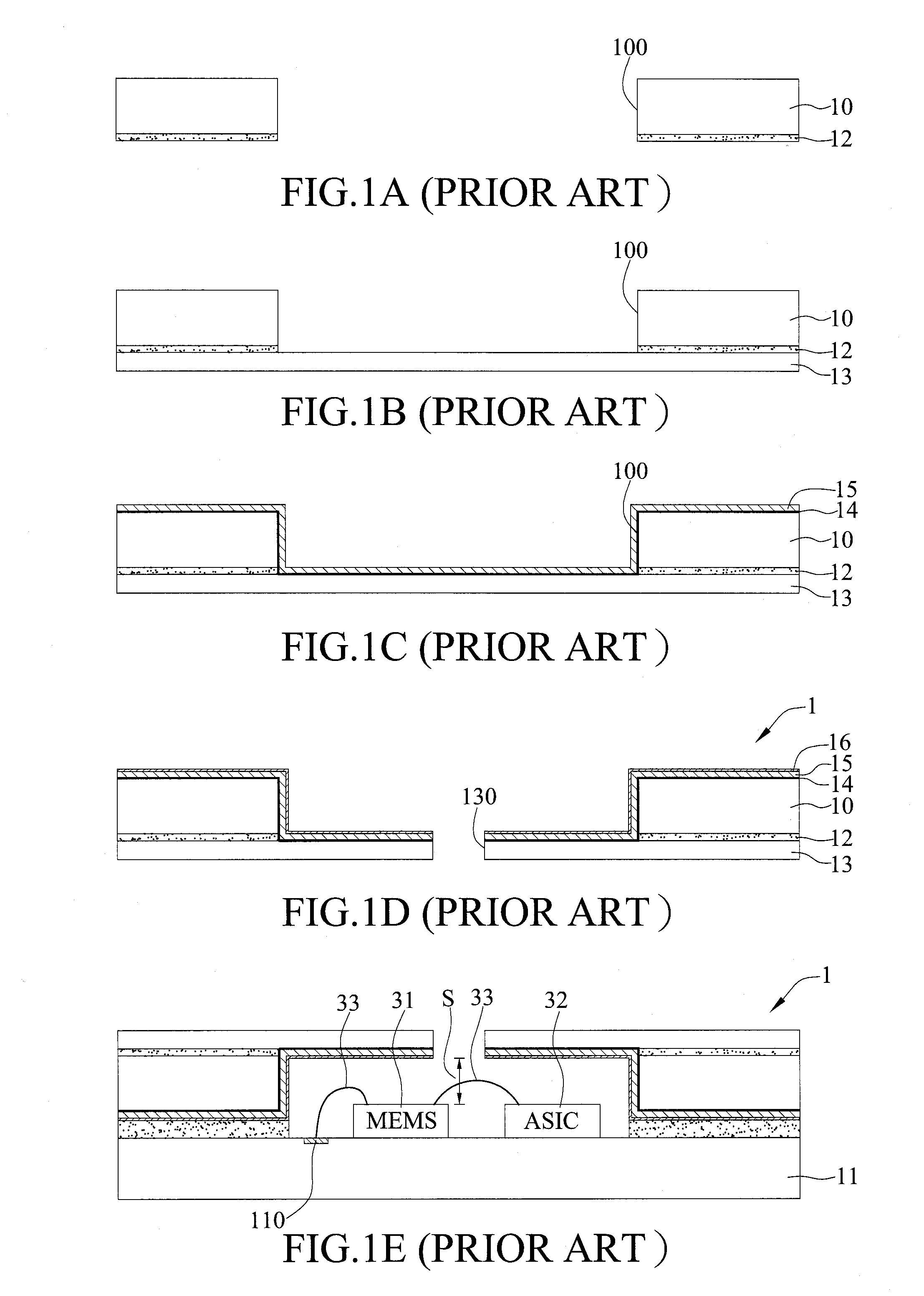
[0032]Referring now to FIGS. 2A through 2I, a method of fabricating an MEMS carrier according to the present invention is illustrated.

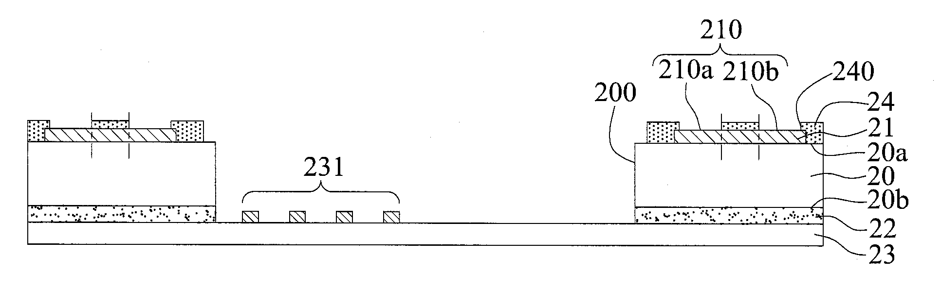
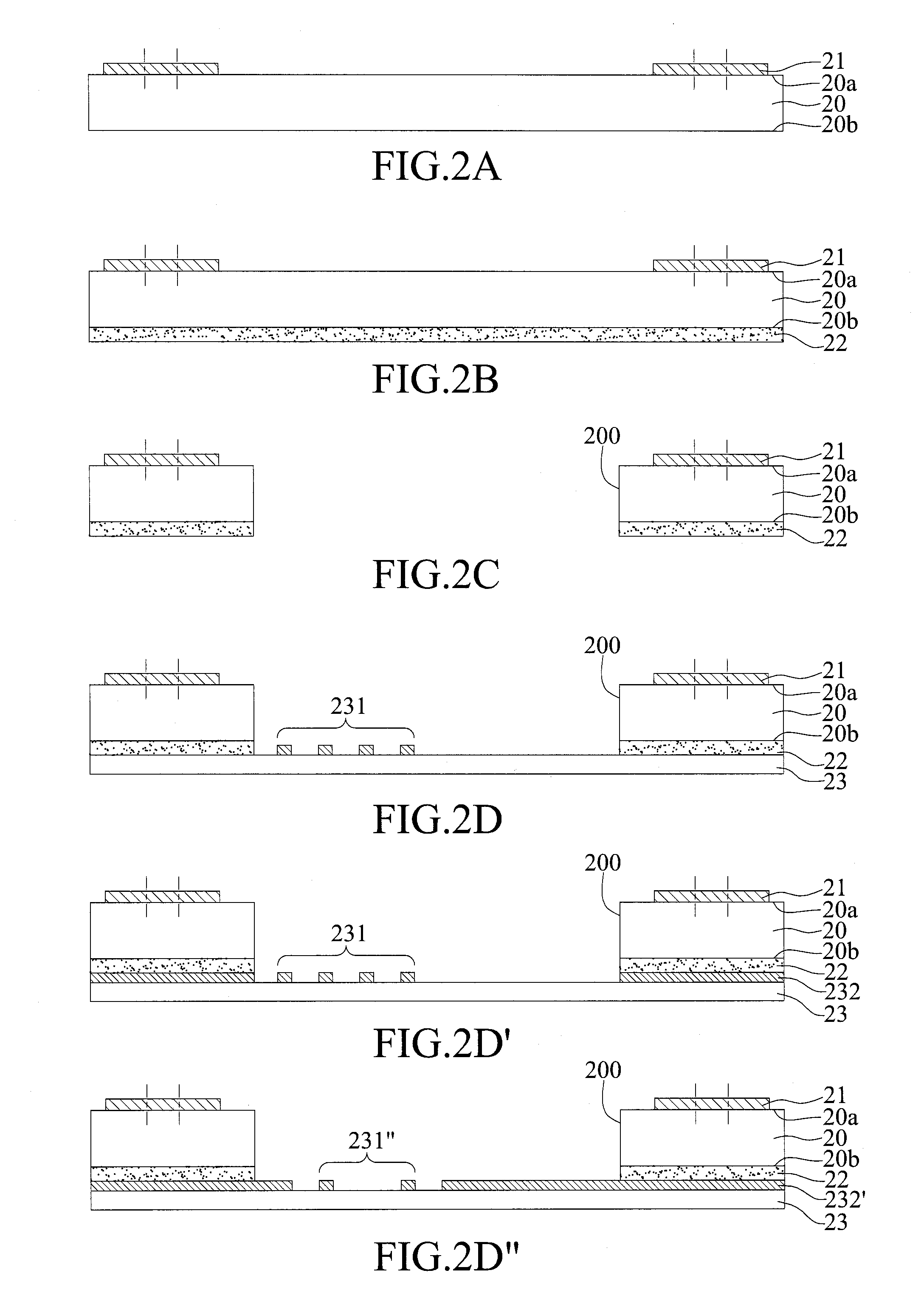
[0033]As shown in FIG. 2A, a core board 20 is provided that has a first surface 20a and an opposite second surface 20b, and a circuit layer 21 is formed on the first surface 20a.

[0034]As shown in FIG. 2B, an adhering layer 22 is formed on the second surface 20b of the core board 20.

[0035]As shown in FIG. 2C, on the core...


PUM


Abstract

An MEMS carrier is provided that includes a core board having a first surface and an opposite second surface, a circuit layer formed on the first surface and having a plurality of conductive pads, and a through hole formed through the first and the second surfaces; a carrier layer formed on the second surface of the core board and covering an end of the through hole; a patterned metal layer formed on a portion of the carrier layer that covers the end of the through hole; a solder mask layer formed on the first surface of the core board and the circuit layer, wherein the solder mask layer has a plurality of openings for exposing the conductive pads; and a shielding metal layer disposed on a sidewall of the through hole, the patterned metal layer, and the portion of the carrier layer that covers the end of the through hole. Without the use of a circuit board, the MEMS carrier has reduced height and size.

Description

BACKGROUND OF THE INVENTION[0001]1. Field of the Invention[0002]This invention relates to carriers and methods of fabricating the same, and, more particularly, to a microelectromechanical system (MEMS) carrier and a method of fabricating the same.[0003]2. Description of Related Art[0004]Nowadays, MEMS devices such as microphones have been broadly used in the mobile communication equipment, audio message device, etc. In order to protect an MEMS device, a cover component is disposed thereon to prevent the MEMS device from being exposed and damaged.[0005]Referring to FIGS. 1A through 1E, cross-sectional diagrams depicting a method of disposing a cover component 1 on an MEMS device according to the prior art are shown.[0006]As shown in FIG. 1A, a core board 10 is provided that has at least a through hole 100 formed through the core board 10, and an adhering layer 12 is formed on a surface of the core board 10.[0007]As shown in FIG. 1B, a carrier layer 13 is adhered to the adhering layer...

Claims


Application Information

Patent Timeline
Patent Type & Authority Applications(United States)
IPC IPC(8): H01L29/84H01L21/02
CPCB81B7/0064B81B2201/0257H01L2224/48091H01L2224/48137H01L2924/1461H01L2924/3025H01L2924/00014H01L2924/00
Inventor TSAI, KUN-CHEN
Owner UNIMICRON TECH CORP
Why Eureka
Try Eureka