

Use of contacts to create differential stresses on devices
a technology of contacts and devices, applied in the direction of semiconductor devices, electrical devices, transistors, etc., can solve the problems of reducing the mobility of carriers and the performance of devices
- Summary
- Abstract
- Description
- Claims
- Application Information
AI Technical Summary
Benefits of technology
Problems solved by technology
Method used
Image

Examples
Embodiment Construction
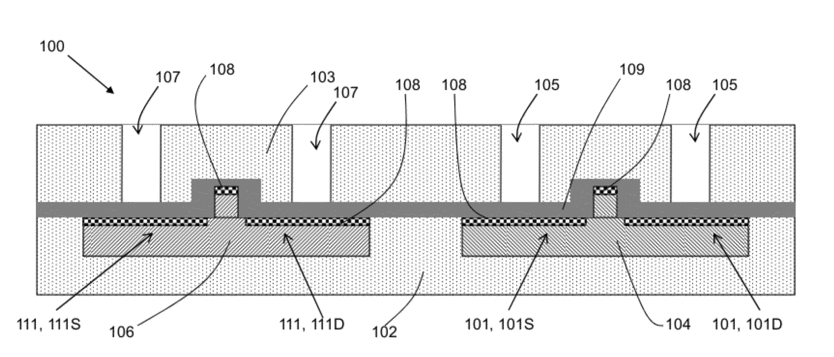
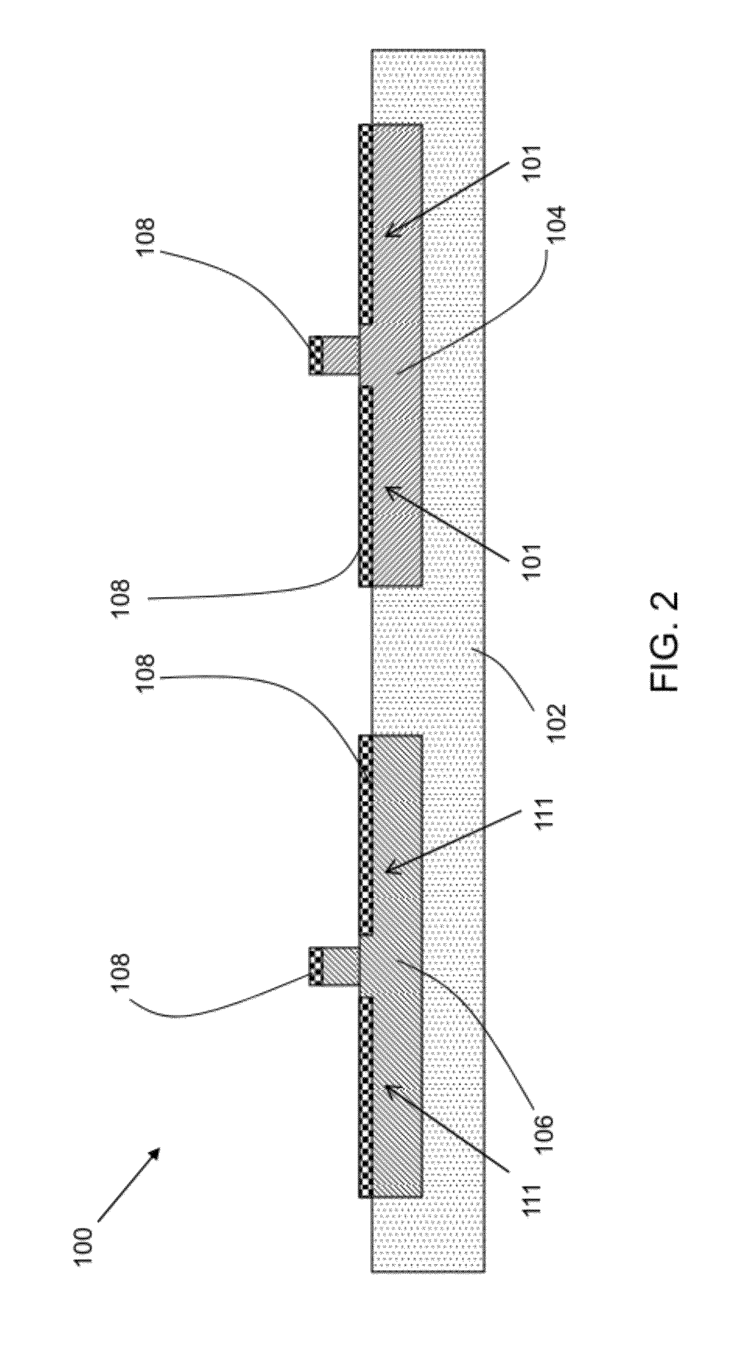
[0014]FIGS. 1-8 show cross-sectional views of one embodiment of a method to create differential stress on a plurality of devices in an integrated circuit (IC) chip 100. FIG. 8 shows IC chip 100 formed as a result of the method shown in FIGS. 1-8.
[0015]Turning to FIG. 1, a substrate 102 is provided. Substrate 102 can be silicon on insulator (SOI) or can be bulk semiconductor material. Substrate 102 includes at least two field effect transistors (FETs), e.g., at least one p-type field effect transistor (PFET) 104 and at least one n-type field effect transistor (NFET) 106. As understood by one of skill in the art, each FET includes a source / drain region, e.g., source / drain regions 101 of PFET 104 and source / drain regions 111 of NFET 106. The details of PFET 104 and NFET 106 are not included in the figures because they are not necessary in order to illustrate the embodiments of the invention disclosed herein, however, one of ordinary skill in the art would understand that PFET 104 and N...
PUM
 Abstract
Description
Claims
Application Information