Liquid crystal display panel

a liquid crystal display and panel technology, applied in optics, instruments, non-linear optics, etc., can solve problems such as color shift and color washout, and achieve the effects of wide viewing angle display, desirable efficiency, and fast response speed

Active Publication Date: 2012-04-12
AU OPTRONICS CORP
View PDF7 Cites 13 Cited by
  • Summary
  • Abstract
  • Description
  • Claims
  • Application Information

AI Technical Summary

Benefits of technology

[0008]The invention is directed to an LCD panel that achieves a wide viewing angle display effect by means of liquid crystal molecules arranged in

Problems solved by technology

That is to say, when the viewing angle is altered, display luminance of th

Method used


Image

  • Liquid crystal display panel
  • Liquid crystal display panel
  • Liquid crystal display panel

Examples


first embodiment

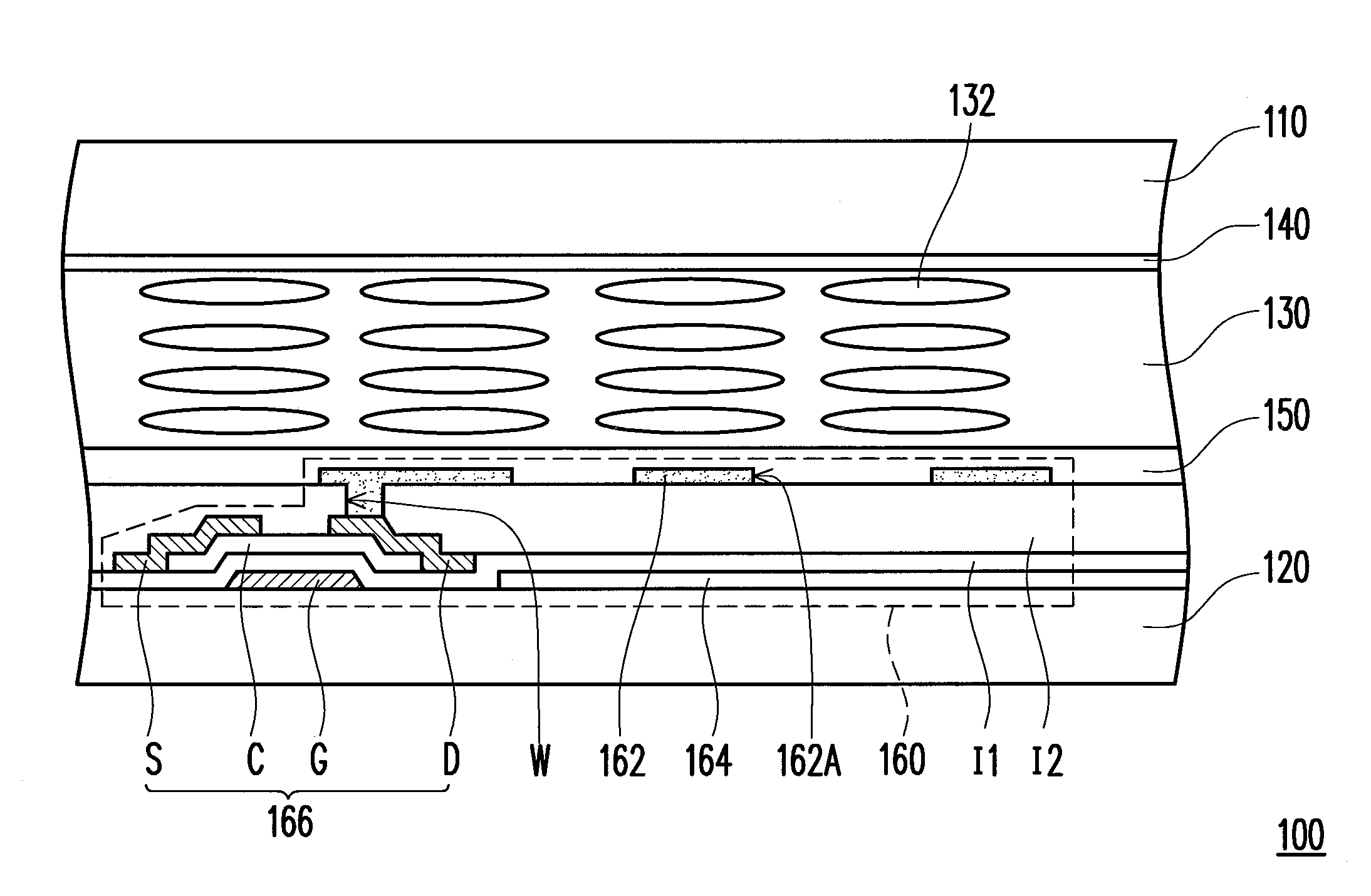
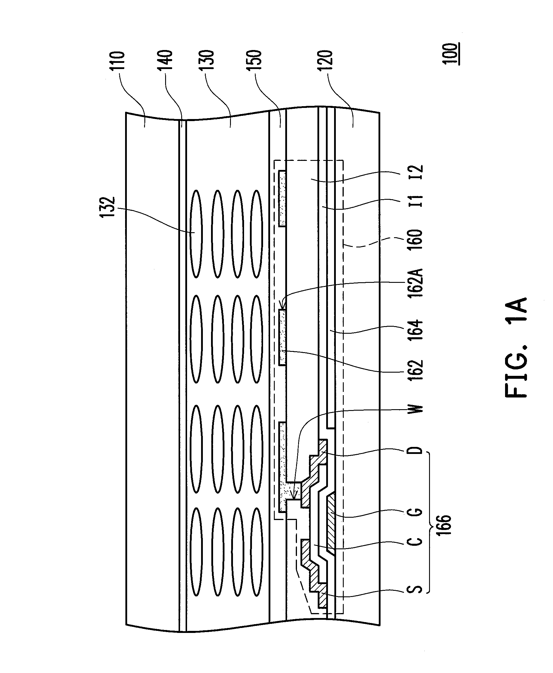
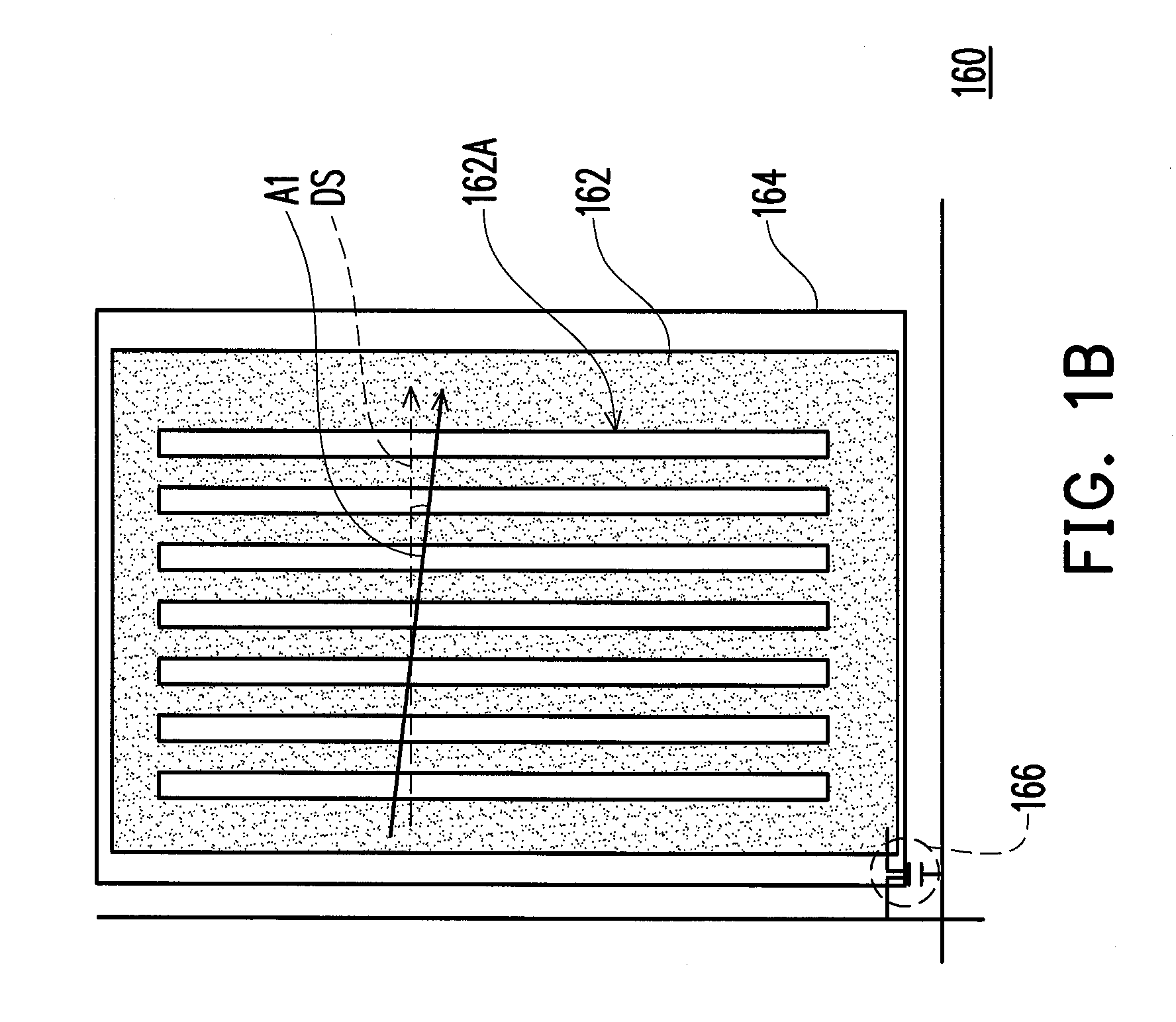
[0028]FIG. 1A is a schematic cross-sectional view illustrating a portion of an LCD panel according to the invention, while FIG. 1B is a schematic top view illustrating an individual pixel structure in the LCD panel depicted in FIG. 1A. With reference to FIG. 1A and FIG. 1B, the LCD panel 100 includes a first substrate 110, a second substrate 120, a PSA liquid crystal layer 130, a first alignment layer 140, a second alignment layer 150, and a plurality of pixel structures 160. Here, only one of the pixel structures 160 is illustrated for explanation, while the number of the pixel structures 160 is plural in the actual design of the LCD panel 100.

[0029]The second substrate 120 is opposite to the first substrate 110 in this embodiment. The PSA liquid crystal layer 130 is configured between the first substrate 110 and the second substrate 120, and liquid crystal molecules 132 of the PSA liquid crystal layer 130 are substantially arranged in parallel to the first substrate 110 and the se...

second embodiment

[0037]In said embodiment, the area occupied by the first common electrode 164 substantially identical to the display area of the entire pixel structure 160 is exemplarily described, while the invention is not limited thereto. FIG. 2 is a schematic cross-sectional view illustrating a portion of an LCD panel according to the invention. With reference to FIG. 2, the LCD panel 200 includes a first substrate 110, a second substrate 120, a PSA liquid crystal layer 130, a first alignment layer 140, a second alignment layer 150, and a pixel structure 260. The relative correlation of these components can be learned from the explanation in the previous embodiment, and therefore no other descriptions are provided herein. The main difference between the LCD panel 100 and the LCD panel 200 of this embodiment lies in that the first common electrode 264 of the pixel structure 260 has a specific pattern and is made of at least one bar-shaped portion 264A. Each of the bar-shaped portions 264A is loc...

sixth embodiment

[0046]The design of the pixel structure is not limited to those described above. FIG. 6A is a schematic cross-sectional view illustrating a portion of an LCD panel according to the invention, while FIG. 6B is a schematic top view illustrating an individual pixel structure in the LCD panel depicted in FIG. 6A. With reference to FIG. 6A and FIG. 6B, the LCD panel 600 includes a first substrate 610, a second substrate 620, a PSA liquid crystal layer 630, a first alignment layer 640, a second alignment layer 650, and a plurality of pixel structures 660. Here, only one of the pixel structures 660 is illustrated for explanation, while the number of the pixel structures 660 is plural in the actual design of the LCD panel 600.

[0047]The second substrate 620 is opposite to the first substrate 610 in this embodiment. The PSA liquid crystal layer 630 is configured between the first substrate 610 and the second substrate 620, and liquid crystal molecules 632 of the PSA liquid crystal layer 630 a...


PUM

PropertyMeasurementUnit
Angleaaaaaaaaaa
Angleaaaaaaaaaa
Angleaaaaaaaaaa

Abstract

A liquid crystal display (LCD) panel includes a first substrate, a second substrate, a polymer stabilized alignment (PSA) liquid crystal layer, a first alignment layer, a second alignment layer, and a plurality of pixel structures. The PSA liquid crystal layer is configured between the first and second substrates, and liquid crystal molecules of the PSA liquid crystal layer are substantially arranged in parallel to the first and second substrates. The first alignment layer is configured between the first substrate and the PSA liquid crystal layer and has a first alignment direction. The second alignment layer is configured between the second substrate and the PSA liquid crystal layer. Each pixel structure is configured between the second substrate and the second alignment layer and has a pixel electrode and a first common electrode. The pixel electrode has at least one slit which is overlapped with the first common electrode.

Description

CROSS-REFERENCE TO RELATED APPLICATION[0001]This application claims the priority benefit of Taiwan application serial no. 99134605, filed on Oct. 11, 2010. The entirety of the above-mentioned patent application is hereby incorporated by reference herein and made a part of this specification.BACKGROUND OF THE INVENTION[0002]1. Field of the Invention[0003]The invention relates to a liquid crystal display (LCD) panel. More particularly, the invention relates to an LCD panel that is characterized by wide viewing angle, and liquid crystal molecules of the LCD panel are arranged in parallel to a substrate in the LCD panel.[0004]2. Description of Related Art[0005]Nowadays, a thin film transistor liquid crystal display (TFT-LCD) panel on the market is required to have high contrast ratio, high luminance, high response speed, and wide viewing angle. Currently, several types of display panels can meet the requirement of wide viewing angles, such as an in-plane switching (IPS) LCD panel, a fri...

Claims


Application Information

Patent Timeline
IPC IPC(8): G02F1/1337
CPCG02F1/134363G02F2001/133738G02F2001/13775G02F2001/13712G02F2001/134372G02F1/133738G02F1/134372G02F1/13712G02F1/13775
Inventor LI, MING-CHUNLU, YING-CHILEE, SEOK-LYUL
Owner AU OPTRONICS CORP
Why Eureka
Try Eureka