Semiconductor apparatus and method of trimming voltage

a technology of semiconductor and voltage, which is applied in the direction of transmission system, process and machine control, instruments, etc., can solve the problems of difficult to generate optimal and common internal voltage vin

Active Publication Date: 2012-05-03
SK HYNIX INC
View PDF3 Cites 15 Cited by
  • Summary
  • Abstract
  • Description
  • Claims
  • Application Information

AI Technical Summary

Problems solved by technology

However, since the semiconductor apparatus of FIG. 2 commonly transfers the internal voltage VINT generated from the master chip MASTER CHIP to the plurality of slave chips SLAVE CHIP1 to SLAVE CHIP4, it is difficult to generate an optimal and common internal voltage VINT that can thoroughly compensate the variation of the process of the respective slave chips SLAVE CHIP1 to SLAVE CHIP4.

Method used


Image

  • Semiconductor apparatus and method of trimming voltage
  • Semiconductor apparatus and method of trimming voltage
  • Semiconductor apparatus and method of trimming voltage

Examples


Embodiment Construction

[0028]Reference will now be made in detail to the exemplary embodiments consistent with the present disclosure, examples of which are illustrated in the accompanying drawings. Wherever possible, the same reference characters will be used throughout the drawings to refer to the same or like parts.

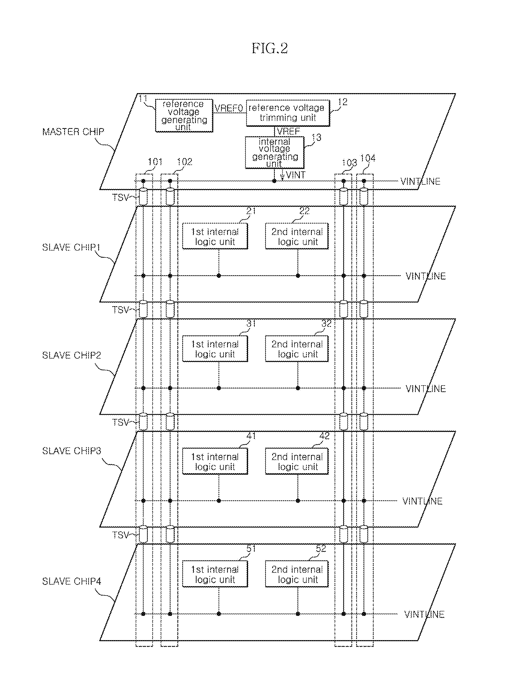
[0029]FIG. 3 is a diagram showing a configuration of a semiconductor apparatus according to one embodiment.

[0030]The semiconductor apparatus in accordance with the present embodiment includes only a simplified configuration for the sake of clear description.

[0031]Referring to FIG. 3, the semiconductor apparatus includes a master chip MASTER CHIP and a plurality of slave chips SLAVE CHIP1 to SLAVE CHIP4. The master chip MASTER CHIP and the plurality of slave chips SLAVE CHIP1 to SLAVE CHIP4 are vertically stacked one on top of another, and a through-silicon via (TSV) 101A is penetrating and electrically coupling the master chip MASTER CHIP and the plurality of slave chips SLAVE CHIP1 to SLAVE...


PUM


Abstract

A semiconductor apparatus includes: a master chip and at least one slave chip configured to be stacked one on top of another; and a through-silicon via (TSV) configured to penetrate and electrically couple the master chip and the at least one slave chip, wherein the at least one slave chip receives a reference voltage generated from the master chip via the TSV and independently trims the reference voltage and then generates an internal voltage with the trimmed reference voltage.

Description

CROSS-REFERENCES TO RELATED APPLICATION[0001]The present application claims priority under 35 U.S.C. §119(a) to Korean application number 10-2010-0106804, filed on Oct. 29, 2010 which is incorporated by reference in its entirety as if set forth in full.BACKGROUND OF THE INVENTION[0002]1. Technical Field[0003]Embodiments relate to a semiconductor apparatus, and more particularly, to a technique for constituting an internal power supply voltage circuit of the semiconductor apparatus having a configuration that a plurality of semiconductor chips are stacked one on top of another.[0004]2. Related Art[0005]A semiconductor apparatus typically receives an external power supply voltage to generate an internal voltage having various voltage levels, and operates an internal circuit of the semiconductor apparatus by using the internal voltage.[0006]FIG. 1 is a block diagram showing a configuration of a power supply voltage generating unit of a typical semiconductor apparatus.[0007]Referring to...

Claims


Application Information

Patent Timeline
Patent Type & Authority Applications(United States)
IPC IPC(8): G05F1/10
CPCG05F1/56H01C17/22Y10T307/305
Inventor IM, JAE HYUK
Owner SK HYNIX INC
Why Eureka
Try Eureka