

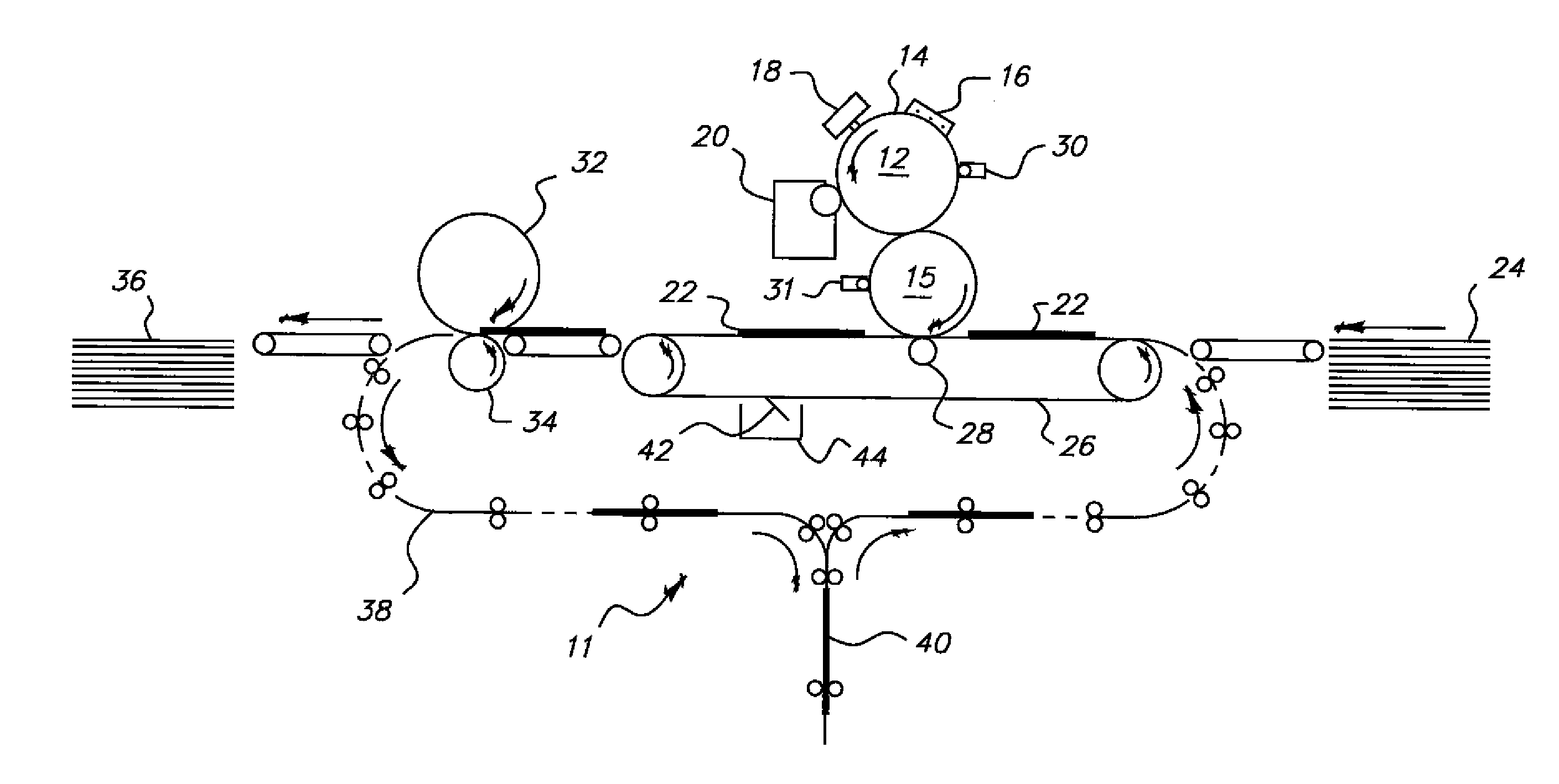
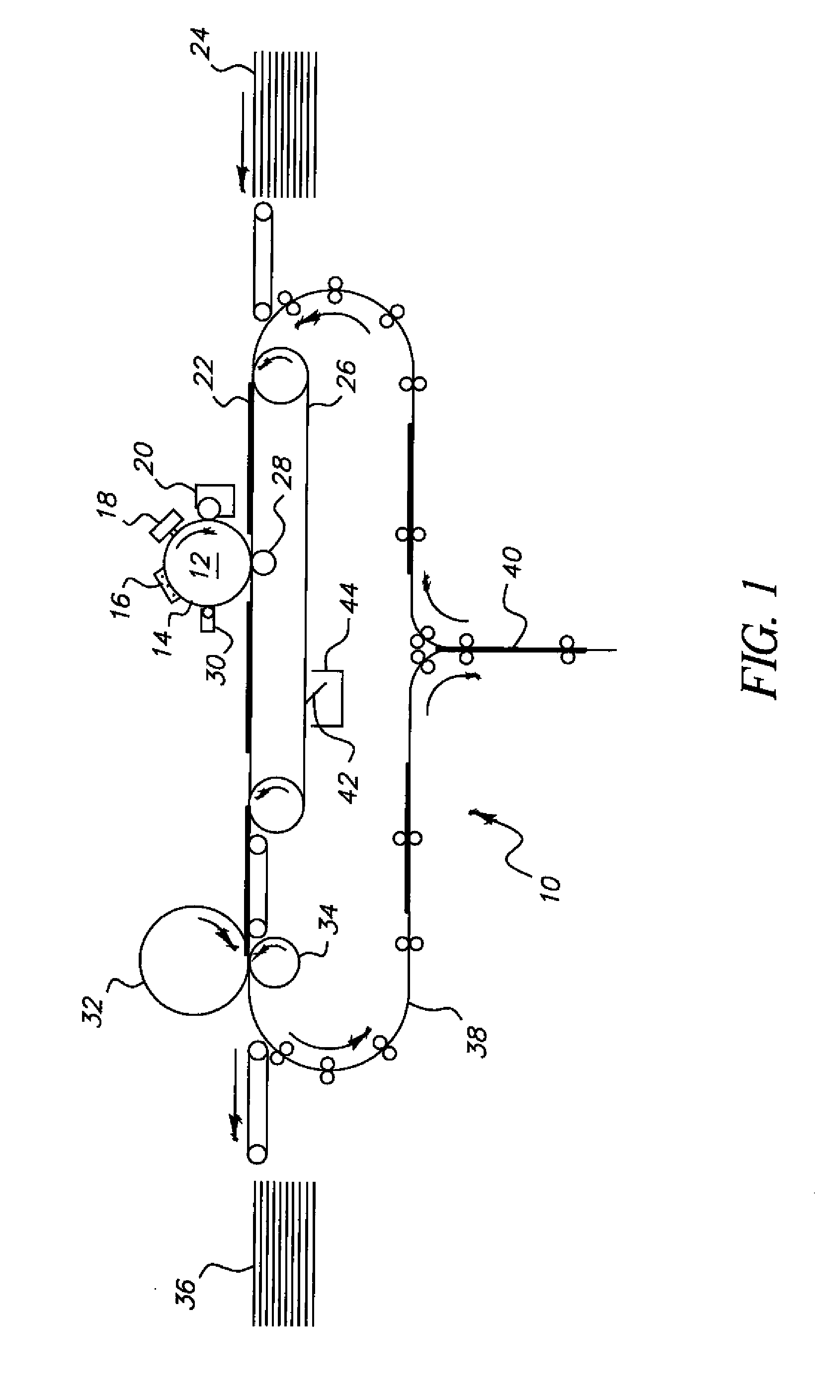
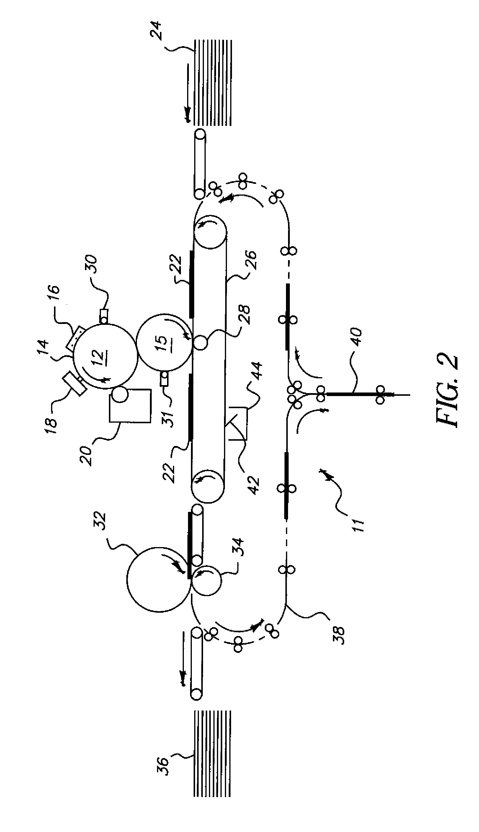
Printed electronic circuit boards and other articles having patterned conductive images
a technology of printed electronic circuit boards and printed circuits, applied in the direction of dielectric characteristics, thermoplastic polymer dielectrics, instruments, etc., can solve the problems of high initial cost and much more layout effor
- Summary
- Abstract
- Description
- Claims
- Application Information
AI Technical Summary
Benefits of technology
Problems solved by technology
Method used
Image

Examples
example 1
[0071]Conducting toner was prepared as described above using silver powder and polyester. The toner was mixed with a ferrite carrier to make a developer and 12 g were loaded onto the shell of a sumpless magnetic electrophotographic development station comprising a core of 20 magnets with alternating poles. An electrostatic latent image comprising lines approximately 0.5 mm across was formed on a photoreceptor and the photoreceptor brought into close proximity with the development station. The developed image was electrostatically transferred to paper and the resulting image fused by exposing to the vapors of dimethyl chloride. The electrical resistance measured between two points approximately 1 inch apart on one of the lines was found to be approximately 100 Ω.
example 2
[0072]Similar to example 1 except that the image was fused in an oven. The electrical resistance was similar.
example 3
[0073]This Example is similar to example 2 except that, after oven fusing, the circuit was placed on a hot plate and heated to approximately 100° C. A sheet of Kaptan-H was placed over the circuit and the Kaptan-H was then manually pressed against the circuit, thereby ferrotyping it. After cooling, the Kaptan-H and the circuit were separated. The resistivity decreased to a few tens of ohms.
PUM
| Property | Measurement | Unit |
|---|---|---|
| glass transition temperature | aaaaa | aaaaa |
| glass transition temperature | aaaaa | aaaaa |
| size | aaaaa | aaaaa |
Abstract
Description
Claims
Application Information