Image display device

Inactive Publication Date: 2012-06-07
HITACHI DISPLAYS +1
View PDF0 Cites 1 Cited by
  • Summary
  • Abstract
  • Description
  • Claims
  • Application Information

AI Technical Summary

Benefits of technology

[0010]The present invention has been made under such circumstances, and it is an object of the present invention to provide an image display device where it is possible to suppress the fluctuation of a potential for light emission caused by a change in an amount of current which flows to a light emitting element.
[0022]According to the present invention, in the image display device, it is possible to suppress the fluctuation of a potential for light emission caused by a change in an amount of current which flows to the light emitting elements.

Problems solved by technology

In such a case, a potential for light emission may fluctuate thus also bringing about the deterioration of image quality or the like.

Method used


Image

  • Image display device
  • Image display device
  • Image display device

Examples


first embodiment

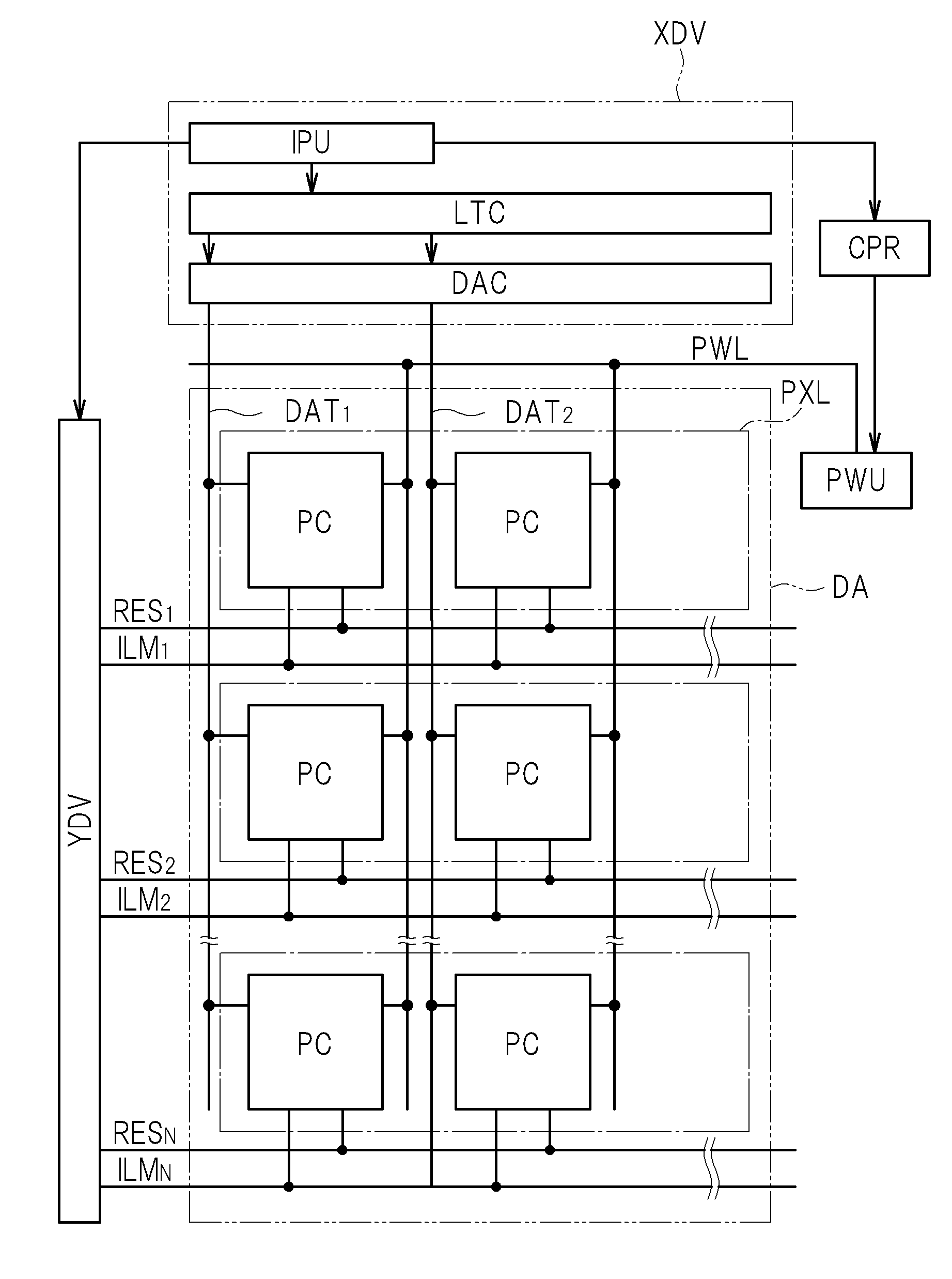
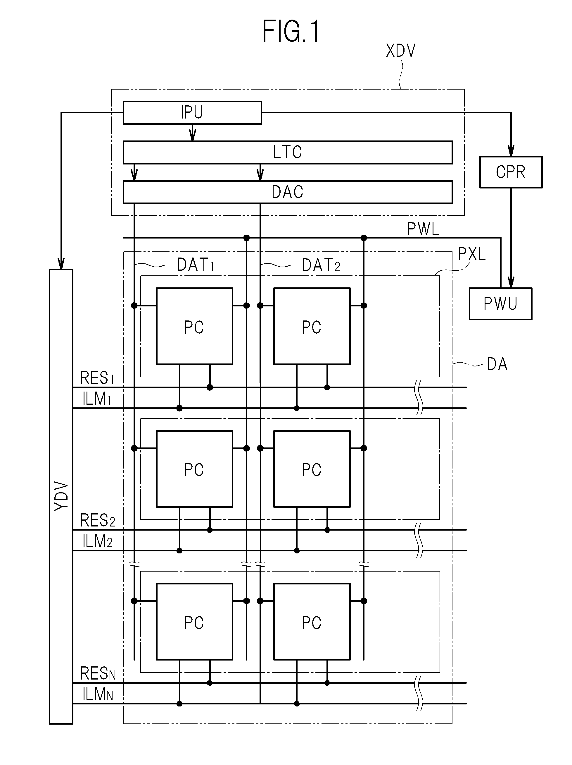
[0043]The organic EL display device physically includes an array substrate, a flexible printed circuit board, and a driver integrated circuit which is sealed in a package. A display region DA where an image is displayed is arranged on the array substrate. FIG. 1 shows one example of the circuit constitution of the organic EL display device according to the first embodiment. The circuit shown in FIG. 1 is mainly provided to the array substrate and the driver integrated circuit. The display region DA is provided above the array substrate of the organic EL display device, and pixel circuits PC are arranged in the display region DA in a matrix array. Assume that the organic EL display device performs a color display with resolution of M rows and N columns, ((3×M) columns×N rows) pieces of pixel circuits PC are arranged within a display region. Here, the row of pixel circuits PC is referred to as a pixel row PXL.

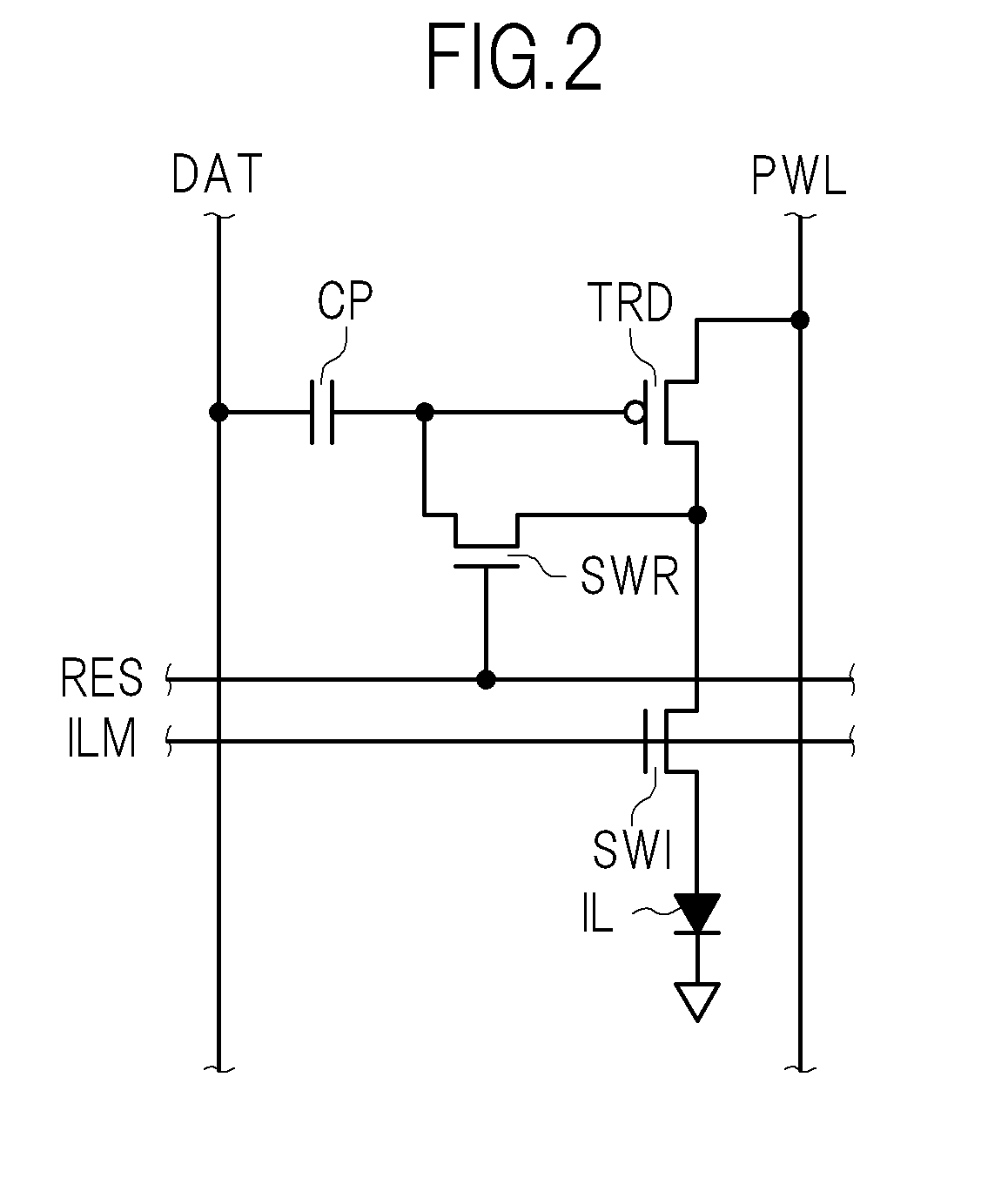
[0044]Within the display region DA, a data line DAT extends in the vertical ...

second embodiment

[0075]The second embodiment relates to a case where the light emitting period TIL starts immediately after a writing operation of a display signal to pixel circuits PC included in each pixel row PXL is finished, and start timing and finish timing of the light emitting period TIL differ for every pixel row PXL. Hereinafter, this embodiment is explained by focusing on points where this embodiment differs from the first embodiment.

[0076]FIG. 14 is a view showing one example of the constitution of each pixel circuit PC of an organic EL display device according to the second embodiment. Each pixel circuit PC includes a light emitting element IL, a drive transistor TRD, a storage capacitor CP, a lighting control switch SWI, a reset switch SWR, a data line input switch SWS, and a light emitting signal input switch SWF. A cathode of the light emitting element IL is connected to a ground potential supply line not shown in the drawing. The drive transistor TRD is a p-channel type thin film tr...


PUM


Abstract

An image display device includes plural pixel circuits each of which includes a light emitting element where an amount of light emission changes corresponding to an amount of current and a drive transistor which controls the amount of current which flows to the light emitting element based on a display signal, a data line drive circuit which supplies a display signal to the plural pixel circuits respectively based on image data, a power source part which outputs a light-emitting potential, and a current amount prediction part which calculates an amount of current which flows to the plural pixel circuits from the power source part based on the image data. The power source part performs a control for suppressing fluctuation of the light-emitting potential based on the calculated amount of current and the outputted light-emitting potential.

Description

CROSS-REFERENCE TO RELATED APPLICATION[0001]The present application claims priority from Japanese application JP2010-271803 filed on Dec. 6, 2010, the content of which is hereby incorporated by reference into this application.BACKGROUND OF THE INVENTION[0002]1. Field of the Invention[0003]The present invention relates to an image display device, and more particularly to an image display device using light emitting elements.[0004]2. Description of the Related Art[0005]Recently, the development of an image display device which uses light emitting elements such as an organic EL display device has been vigorously underway. Plural pixel circuits are arranged in a display region of an image display device, and each pixel circuit includes a light emitting element. A power source circuit which generates a potential for light emission is provided for supplying an electric current for making respective light emitting elements emit light.[0006]FIG. 19 shows an example of the constitution of a ...

Claims


Application Information

Patent Timeline
IPC IPC(8): G09G5/10
CPCG09G3/3233G09G2300/0819G09G2330/028G09G2320/0233G09G2300/0833
Inventor YOKOYAMA, JUNICHITSUKAHARA, MASAHISAAKIMOTO, HAJIME
Owner HITACHI DISPLAYS
Why Eureka
Try Eureka