Monochromatic light source

Inactive Publication Date: 2011-06-23
3M INNOVATIVE PROPERTIES CO
View PDF33 Cites 25 Cited by
  • Summary
  • Abstract
  • Description
  • Claims
  • Application Information

AI Technical Summary

Benefits of technology

[0005]In another embodiment, a light emitting system includes an electroluminescent device that emits light at a first wavelength. The light emitting system further includes an optical cavity that enhances emission of light from a top surface of the light emitting system and suppresses emission of light from one or more sides of the light emitting system. The optical cavity includes a semiconductor multilayer stack that receives the emitted first wavelength light and converts at least a portion of the received light to light of a second wavelength. The semiconductor multilayer stack includes a II-VI potential well. The integrated emission intensity of all light at the second wavelength that exit the light emitting system is at least 10 times the integrated emission intensity of all light at the first wavelength that exit the light emitting system. In some cases, the II-VI potential well includes Cd(Mg)ZnSe or ZnSeTe. In some cases, the electroluminescent device is so designed that a substantial portion of the first wavelength light that is received by the semiconductor multilayer stack, exits the electroluminescent device through a top surface of the electroluminescent device. In some cases, light that is emitted by the light emitting system along a first direction has a first set of color coordinates and light that is emitted by the light emitting system along a second direction different than the first direction has a second set of color coordinates, where the second set of color coordinates is substantially the same as the first set of color coordinates. In some cases, the first set of color coordinates are u1′ and v1′ and the second set of color coordinates are u2′ and v2′, and the absolute value of each of differences between u1′ and u2′ and between v1′ and v2′ is no more than 0.003. In some cases, a primary portion of the re-emitted second wavelength light exits the light emitting system from a top surface of the light emitting system. The top surface has a minimum lateral dimension Wmin. A substantial fraction of the remaining portion of the re-emitted second wavelength light exits the light emitting system from one or more sides of the optical cavity that have a maximum edge thickness Tmax. The ratio Wmin / Tmax is at least about 30. A primary portion of the emitted first wavelength light exits the electroluminescent device from a top surface of the electroluminescent device. The top surface has a minimum lateral dimension W1min. The remaining portion of the emitted first wavelength light exits the electroluminescent device from one or more sides of the electroluminescent device that have a maximum edge thickness T1max. The ratio W1min / T1max is at least about 30. In some cases, each of the ratios Wmin / Tmax and W1min / T1max is at least about 100.

Problems solved by technology

In other regions of the spectrum, however, known laser diodes, such as frequency doubled laser diodes, are complicated, bulky, inefficient, and expensive.

Method used


Image

  • Monochromatic light source
  • Monochromatic light source
  • Monochromatic light source

Examples


Embodiment Construction

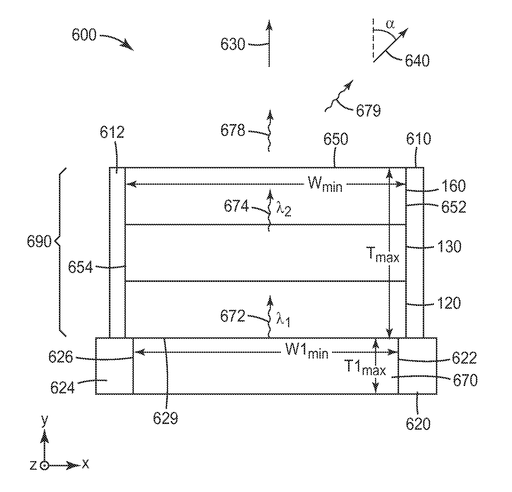
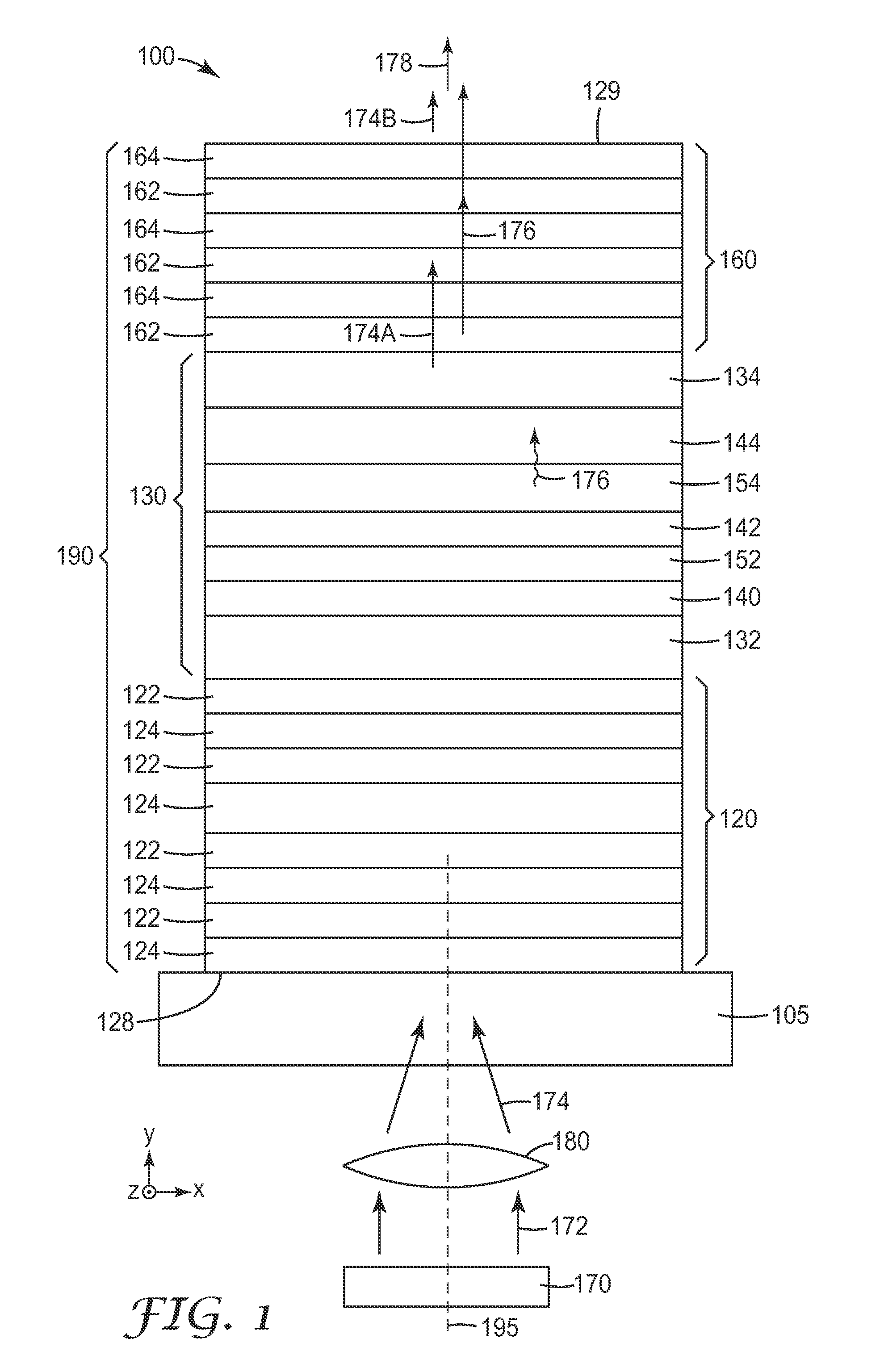
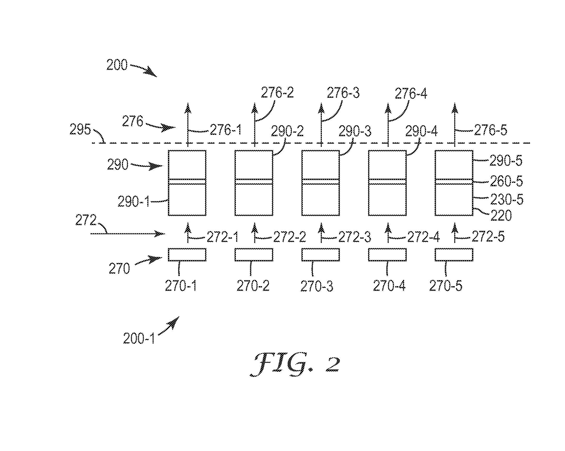
[0015]This application discloses semiconductor light sources that include one or more pump light sources and one or more semiconductor optical cavities for converting light emitted by a pump light source to a different wavelength light. In some cases, a disclosed semiconductor optical cavity is a resonant-cavity capable of converting, such as down converting, an incident light. In some cases, a disclosed semiconductor resonant-cavity wavelength converter is a vertical cavity surface emitting laser (VCSEL). The disclosed light sources are efficient, compact, and in some cases, inexpensively integrate a light converting VCSEL with a pump light source from two or more different semiconductor groups. For example, this application discloses a light source that integrates a III-V pump light source, such as a pump light source that includes N, such as a AlGaInN pump LED or a laser diode, with a II-VI VCSEL that includes a II-VI semiconductor wavelength converter, such as a Cd(Mg)ZnSe wavel...


PUM


Abstract

Light emitting systems are disclosed. The light emitting system includes an electroluminescent device that emits light at a first wavelength. The light emitting system further includes an optical cavity that enhances emission of light from a top surface of the light emitting system and suppresses emission of light from one or more sides of the light emitting system. The optical cavity includes a semiconductor multilayer stack that receives the emitted first wavelength light and converts at least a portion of the received light to light of a second wavelength. The semiconductor multilayer stack includes a II-VI potential well. The integrated emission intensity of all light at the second wavelength that exit the light emitting system is at least 10 times the integrated emission intensity of all light at the first wavelength that exit the light emitting system.

Description

FIELD OF THE INVENTION[0001]This invention generally relates to semiconductor light sources. The invention is particularly applicable to semiconductor light sources that include one or more II-VI semiconductor compounds.BACKGROUND[0002]Laser diodes are used in many different applications such as laser pointers, projection displays, and sensors. Laser diodes that emit in the near UV, violet, near infrared, or infrared regions of the spectrum can be compact and inexpensive. In other regions of the spectrum, however, known laser diodes, such as frequency doubled laser diodes, are complicated, bulky, inefficient, and expensive. There is a great need for a compact, efficient, and inexpensive laser diode system capable of emitting at other desirable wavelengths, such as in the cyan, green, charteuse, yellow and amber regions of the spectrum.SUMMARY OF THE INVENTION[0003]Generally, the present invention relates to semiconductor light sources. In one embodiment, a light source includes a II...

Claims


Application Information

Patent Timeline
IPC IPC(8): H01S5/347H01L33/00F21V9/40
CPCH01S5/02476H01S5/423H01S5/183H01S5/041H01L33/505H01L33/507
Inventor LEATHERDALE, CATHERINE A.HAASE, MICHAEL A.
Owner 3M INNOVATIVE PROPERTIES CO
Why Eureka
Try Eureka