Solid-state imaging device, driving method thereof, and camera

Inactive Publication Date: 2009-10-29
PANASONIC CORP
View PDF14 Cites 8 Cited by
  • Summary
  • Abstract
  • Description
  • Claims
  • Application Information

AI Technical Summary

Benefits of technology

[0031]Furthermore, the driving method of the solid-state imaging device and the camera of the present invention produce the same advantageous effects as described above.
[0032]According to the above-described configurations, it is possible to keep the current flowing to the signal output unit low and reduce the source-to-drain voltage Vds of the drive transistor of the source-follower circuit included in the signal output unit during the imaging exposure period and the unnecessary-charge sweep-out period, and, during the outputting period excluding the unnecessary-charge sweep-out period of the imaging signal, since the current that causes the signal output unit to operate normally flows, the light emission phenomenon caused by the hot electrons can be suppressed.
[0033]Furthermore, it is possible to keep the current flowing to the signal output unit low also during the unnecessary-charge sweep-out period, and, during the outputting period excluding the unnecessary-charge sweep-out period of the imaging signal, since the current that causes the signal output unit to operate normally flows, it is possible to reduce differences in hot electron light emission phenomena and heat emission suppression effectiveness between respective fields.
[0034]In addition, it is possible to suppress the hot electron light emission phenomenon and the heat emission generated from an internal peripheral circuit such as a bias voltage generating circuit aside from the substrate bias voltage generating circuit which influences the spectral characteristics of photodiodes aside from the signal output unit.
[0035]Furthermore, since the impact of the hot electron light emission phenomenon and the heat emission on images increases when the semiconductor substrate is thin, for example, equal or less than 600 μm, the light-sensing unit which accumulates the signal charge corresponding to the amount of received light, the charge transmission unit which transmits and outputs the signal charge accumulated by the light-sensing unit, and the signal output unit which converts the signal charge transmitted by the charge transmission unit into an imaging signal and outputs the imaging signal, are most effective when provided in a semiconductor substrate equal to or less than 600 μm.FURTHER INFORMATION ABOUT TECHNICAL BACKGROUND TO THIS APPLICATION
[0036]The disclosure of Japanese Patent Application No. 2008-116132 filed on Apr. 25, 2008 including specification, drawings and claims is incorporated herein by reference in its entirety.

Problems solved by technology

However, in the conventional techniques disclosed in Patent Reference 1 and Patent Reference 2, there is the problem of picture quality deterioration due to the light emission phenomenon caused by hot electrons.
Since light emission intensity increases in proportion to the source-to-drain voltage Vds, light emission caused by the hot carrier cannot be suppressed even when the amount of current is reduced.
Thus, since the impact of heat emission is borne more heavily by a more-subsequent field, there is the problem of having differences in effectiveness between fields.

Method used


Image

  • Solid-state imaging device, driving method thereof, and camera
  • Solid-state imaging device, driving method thereof, and camera
  • Solid-state imaging device, driving method thereof, and camera

Examples


first embodiment

[0053]Hereinafter, a solid-state imaging device in a first embodiment of the present invention shall be described with reference to the Drawings.

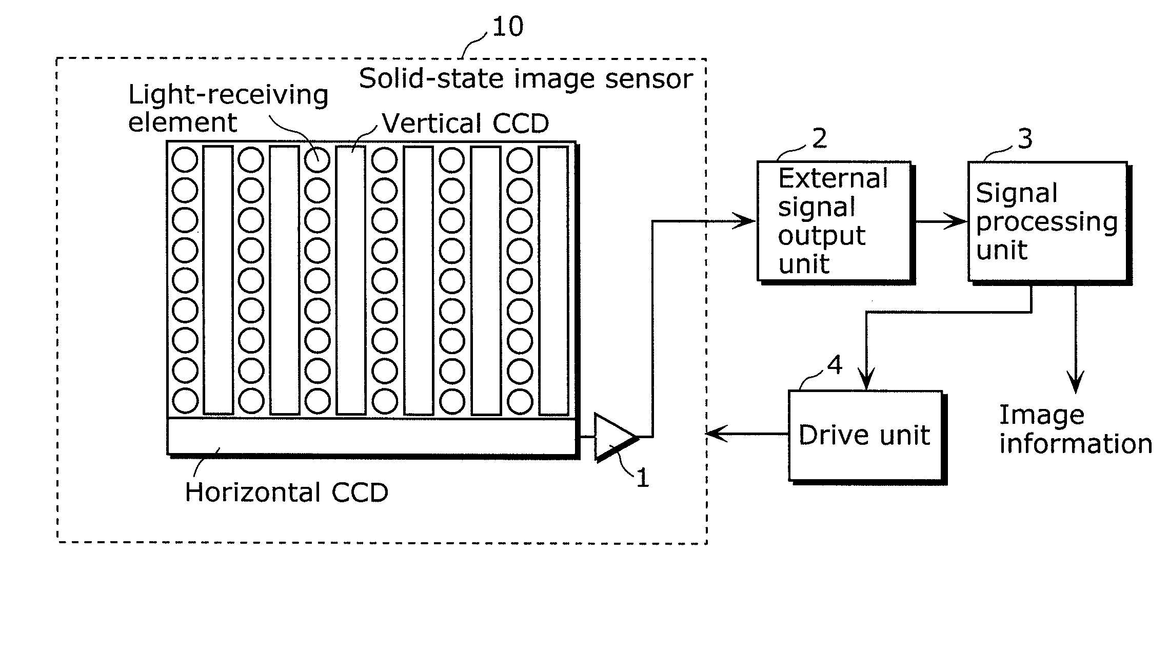
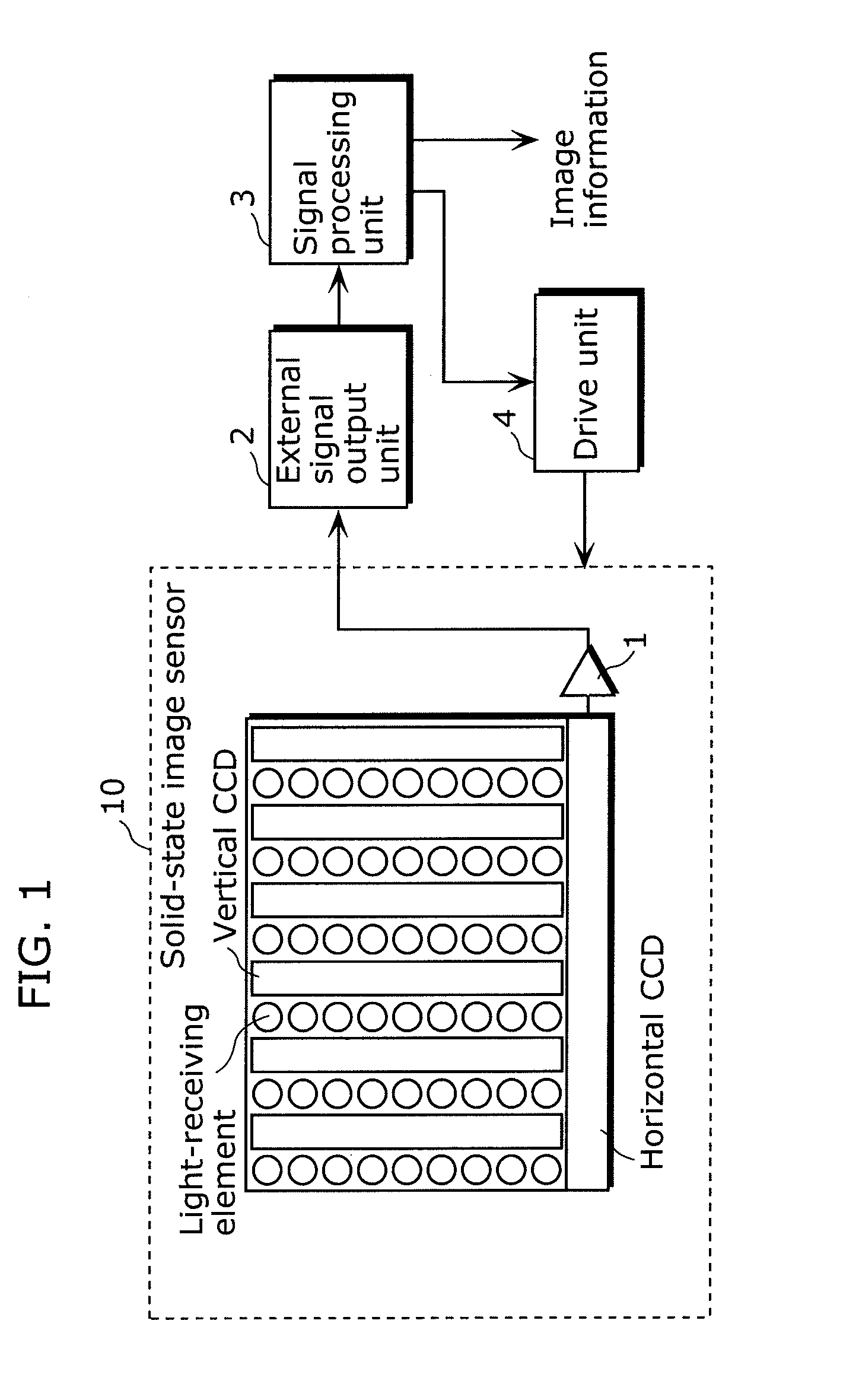
[0054]FIG. 1 is an outline diagram showing the configuration of the solid-state imaging device in a first embodiment of the present invention.

[0055]The solid-state imaging device in the present embodiment is built into the image-capturing device such as a video camera or a digital still camera, and outputs image information by photo-electric conversion of a subject image formed using a lens. As shown in FIG. 1, the solid-state imaging device includes a solid-state image sensor 10, an internal signal output unit 1, an external signal output unit 2, a signal processing unit 3, and a driving unit 4.

[0056]The solid-state image sensor 10 is a semiconductor device that is driven by the driving unit 4, and which outputs, in a predetermined sequence, from the internal signal output unit 1 to the external signal output unit 2, using plural vertical ...

second embodiment

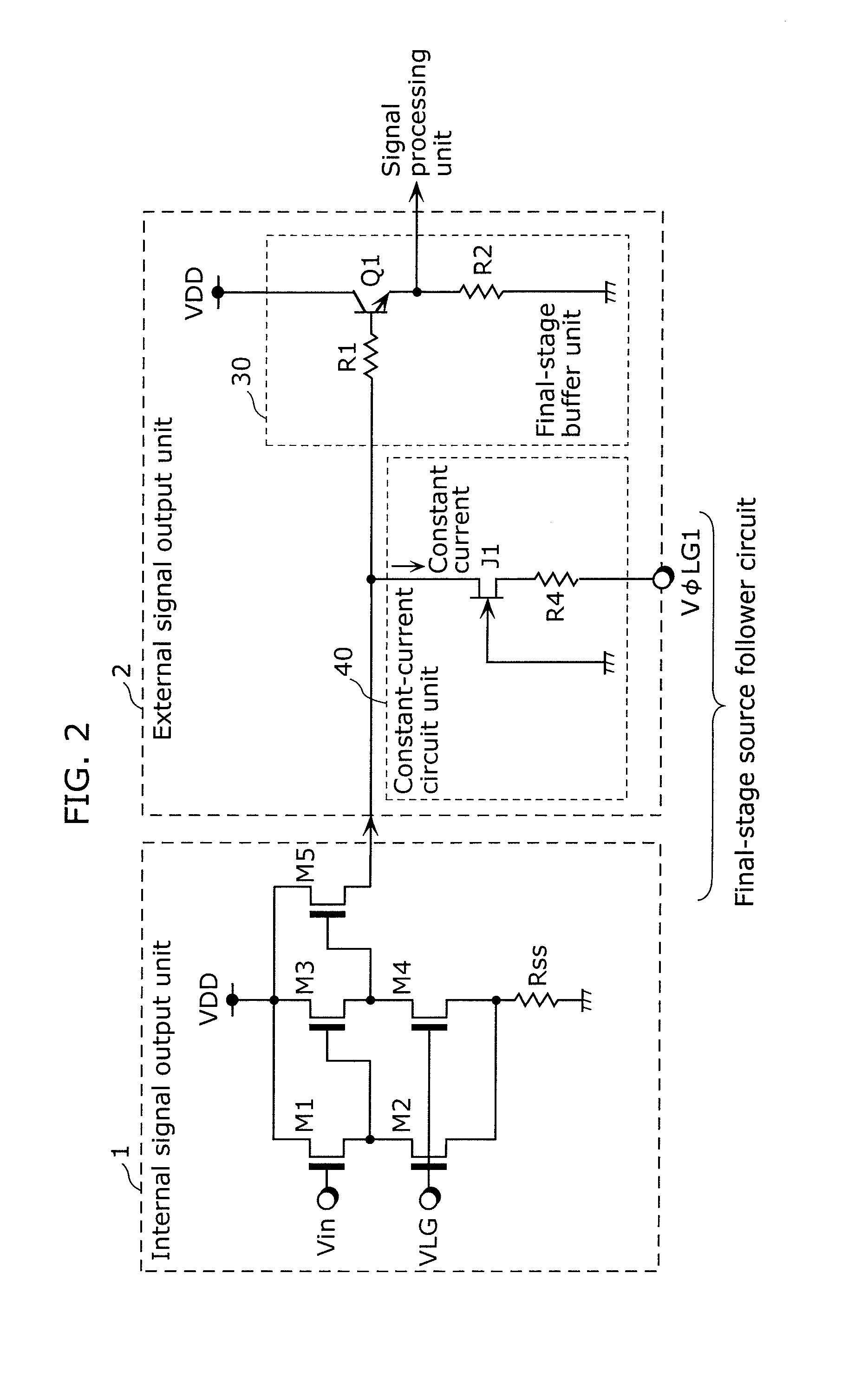
[0095]Hereinafter, a solid-state imaging device in a second embodiment of the present invention shall be described. First, the configuration shown for the solid-state imaging device in the present embodiment is the same as that in FIG. 1 except for the parts described in FIG. 3 to be discussed later.

[0096]Next, FIG. 4 is an outline diagram showing the configuration of a signal output unit of the solid-state imaging device in the second embodiment of the present invention.

[0097]In FIG. 4, the internal signal output unit 1 in a solid-state image sensor including light-receiving elements is configured of three-stages of source follower circuits using the MOS transistors M1 to M5. M1, M3, and M5 are drive transistors and M2 and M4 serve as load transistors which are the current supply units for operating the drive transistors M1 and M3. Furthermore, the drains of the respective drive transistors M1, M3, and M5 are connected to the power terminal VDD. Furthermore, the respective gates of...

third embodiment

[0117]Hereinafter, a solid-state imaging device in a third embodiment of the present invention shall be described.

[0118]FIG. 7 is an outline diagram showing the configuration of the solid-state imaging device in a third embodiment of the present invention. In the diagram, compared to FIG. 1, a solid-state image sensor 11 is included in place of the solid-state image sensor 10. In the solid-state image sensor 11, a peripheral circuit 6 and a bias voltage generating circuit 7, whose description were omitted in the solid-state image sensor 10, are clearly specified. The peripheral circuit 6 is, for example, a timing generator, and generates horizontal transmission pulses Vφ1 to Vφ6, and horizontal pulses Hφ1 and Hφ2. The bias voltage generating circuit 7 generates a bias voltage and supplies this to the peripheral circuit 6.

[0119]It should be noted that the remaining device configuration is the same as in the solid-state imaging device in the second embodiment described using FIG. 4.

[0...


PUM


Abstract

To provide a solid-state imaging device which suppresses light emission caused by hot electrons, and reduces the difference in the impact of heat emission between fields. In the solid-state imaging device in the present invention, the final-stage source-follower circuit within the output circuit includes a drive transistor and a load transistor connected to the drive transistor, and, by applying, to the load transistor, a control signal having different levels for a first period including a charge sweep-out period and an exposure period of the light-receiving elements in a signal outputting period, and a second period which is a period excluding the charge sweep-out period from the signal outputting period, the source-to-drain voltage of the final-stage drive transistor in the first period is made lower than the source-to-drain voltage in the second period.

Description

BACKGROUND OF THE INVENTION[0001](1) Field of the Invention[0002]The present invention relates to a solid-state imaging device, a driving method thereof, and a camera.[0003](2) Description of the Related Art[0004]The demand for Charge-Coupled Device (CCD) solid-state imaging devices as imaging devices in Digital Still Cameras (DSC) or Digital Video Cameras (DVC) is increasing. Furthermore, the addition of a camera function even in mobile terminal apparatuses represented by mobile phones is also being required, and CCD solid-state imaging devices are being widely used.[0005]However, since there is a tendency for dark current of light-receiving elements to increase following a rise in temperature in a CCD solid-state imaging device, there is localized image whitening and the occurrence of shading due to the increase of the dark current of light-receiving elements in the vicinity of a signal output unit, and thus causing image deterioration.[0006]As a countermeasure, as shown in Japane...

Claims


Application Information

Patent Timeline
IPC IPC(8): H04N5/335H04N5/361H04N5/372H04N5/376
CPCH04N5/359H04N5/378H04N5/3728H04N5/372H04N25/62H04N25/73H04N25/71H04N25/75
Inventor MAKIYAMA, KAZUYAKOHNO, AKIYOSHISUZUKI, SEITSUKAMOTO, AKIRA
Owner PANASONIC CORP
Why Eureka
Try Eureka