Method for driving plasma display panel and plasma display device

Inactive Publication Date: 2010-09-09
PANASONIC CORP
View PDF1 Cites 7 Cited by
  • Summary
  • Abstract
  • Description
  • Claims
  • Application Information

AI Technical Summary

Benefits of technology

[0040]According to the present invention, one TV field is composed of a plurality of subfields (SF) and a voltage to the first electrodes in a sustain period of the subfield (SF1) having the smallest brightness weight is smaller than in a sustain period of any SF other than SF1 (feature A) so as to weaken an intensity of a sustain discharge. Accordingly, the light emission brightness in SF1 can be suppressed, thereby lowering the brightness of the 1st gradation level.
[0041]When the voltage applied to the first electrodes in the sustain period is set to be small, as described above, a discharge delay increases in general, hindering a sufficient sustain discharge, and an insufficient sustain discharge in SF1 is likely to cause a reset discharge error in the all-cell reset period. In view of this, the present invention includes one or both of the features B and C described in “Means of Solving the Problems”, allowing a stable reset discharge in the all-cell reset period as a result.
[0042]That is to say, the application of a positive voltage to the third electrodes in the sustain period of SF1 (feature B) facilitates extraction of electrons from the surface of the protective layer of the front panel; Consequently, even if the voltage applied to the first electrodes is rendered smaller, the sustain discharge can still be performed stably. As a result, the reset discharge can be performed stably in the all-cell reset period.
[0043]Also, the application of a positive voltage to the third electrodes in at least part of the voltage rising period of the all-cell reset period (feature C) prevents start of a reset discharge between the first and third electrodes. Consequently, even if the sustain discharge in the previous SF is insufficient, a stable reset discharge can still be performed.
[0044]Although performing one of the features B and C is effective in suppressing reset errors, as described above, performing both of the features B and C can achieve an synergetic effect.
[0045]Thus, by including two or more of the above-mentioned features (A, B, C), an stable reset discharge can be performed even in the case where the voltage applied to the first electrodes in the sustain period of SF1 is set to be further smaller.

Problems solved by technology

However, for plasma display devices (hereinafter, referred to as “PDP devices”), it is difficult to reduce the relative brightness ratio in low gradation levels, and accordingly, it is difficult to achieve smooth expression in low gradation levels.
As a result, unlike CRTs, it is difficult for PDPs to express brightness variation smoothly.
Additionally, because a peak brightness of PDPs is low in the first place, a virtual gradation display using error diffusion processing (dither method) accentuates roughness due to error diffusion noises in an image, deteriorating the image on the contrary as a result of being unable to achieve an error diffusion effect.

Method used


Image

  • Method for driving plasma display panel and plasma display device
  • Method for driving plasma display panel and plasma display device
  • Method for driving plasma display panel and plasma display device

Examples


first embodiment

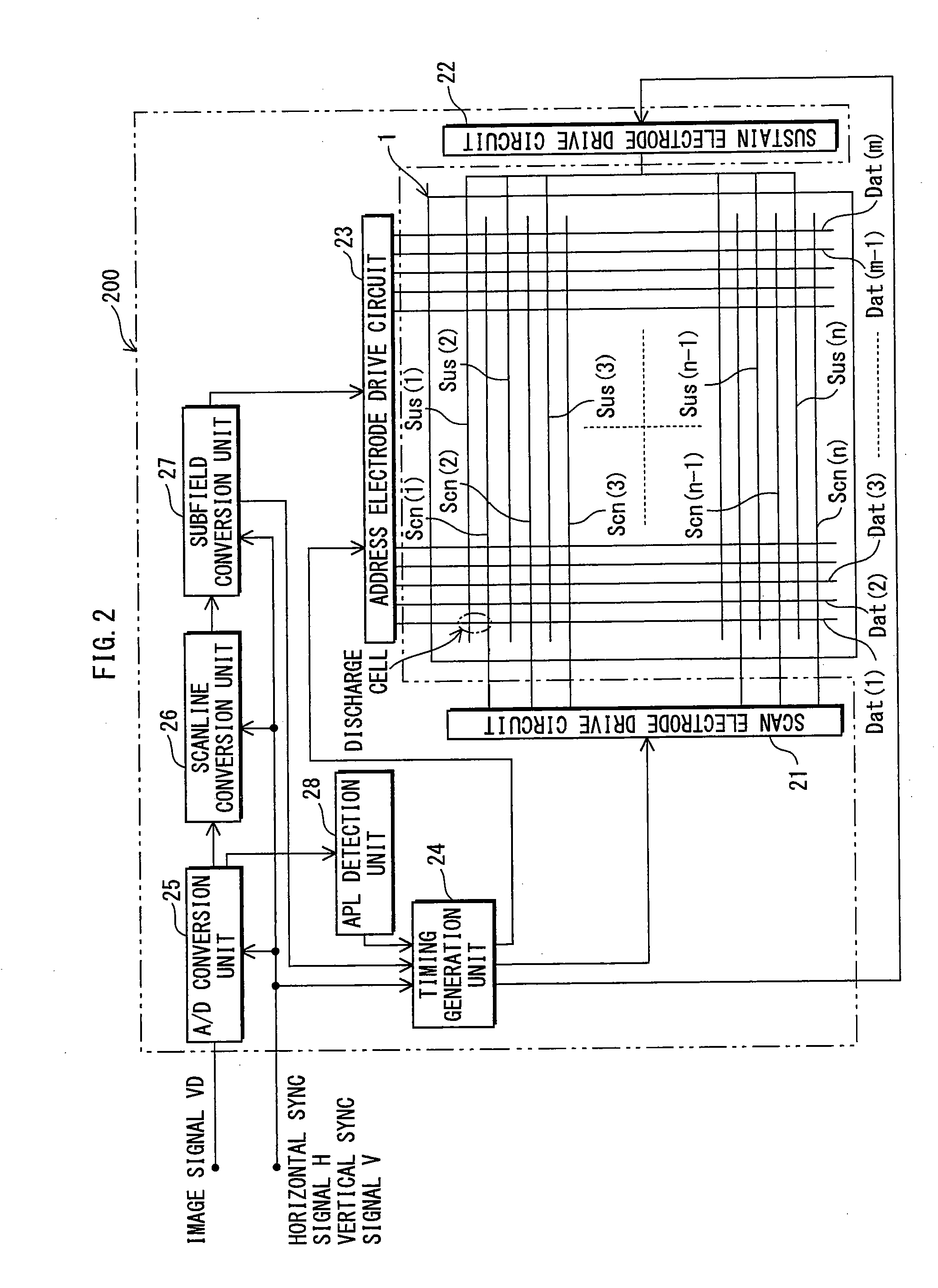
[0086]The PDP device includes a PDP and a drive unit.

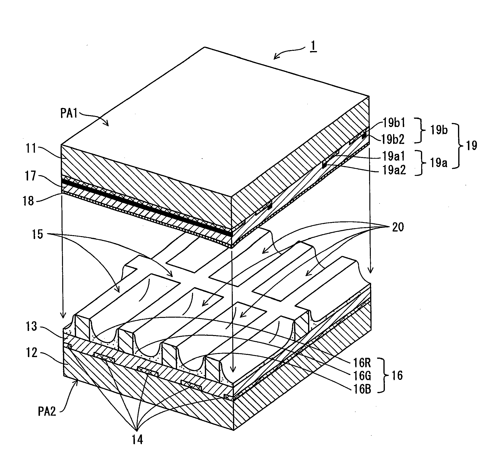
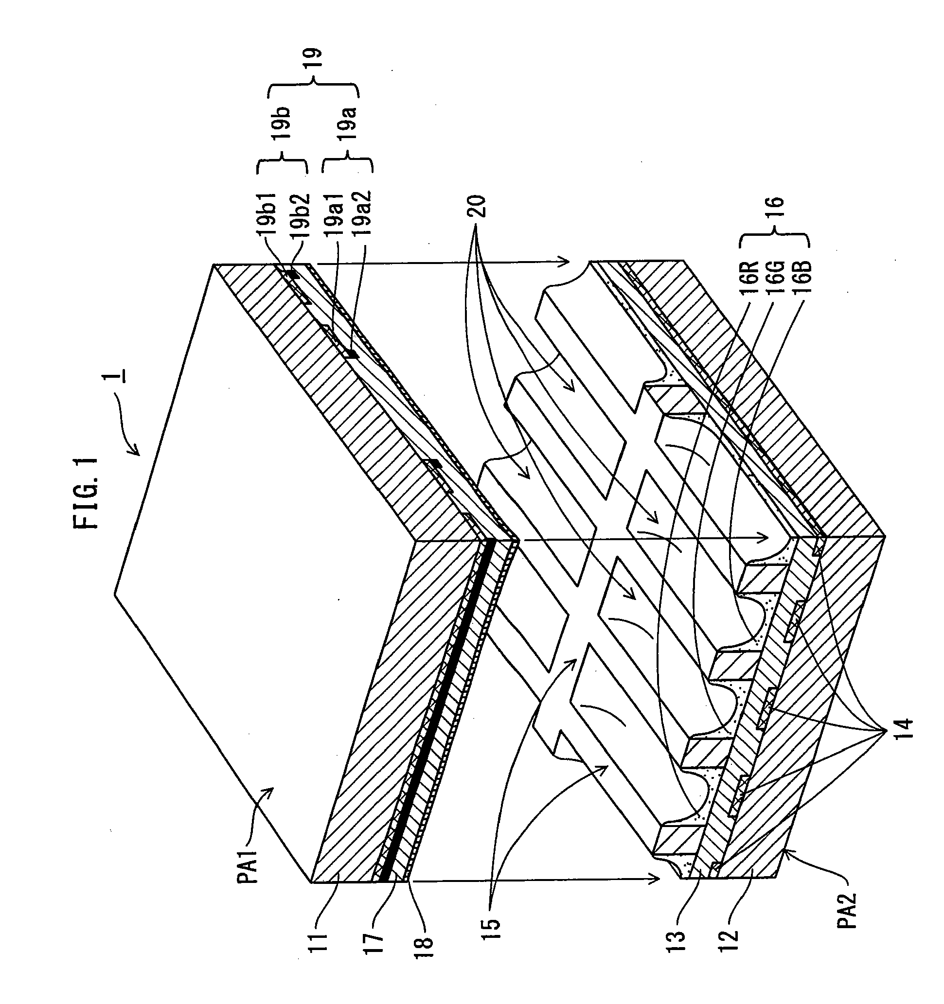
[0087]FIG. 1 shows a structure of a PDP 1 of the present embodiment.

[0088]The PDP 1 is composed of a front panel PA1 and a back panel PA2 opposing each other.

[0089]The front panel PA1 includes a front glass substrate 11 on which display electrode pairs 19 each composed of a scan electrode 19a as a first electrode and a sustain electrode 19b as a second electrode are formed in a stripe pattern, and a dielectric layer 17 and a protective layer 18 are formed to cover the scan electrodes 19a and the sustain electrodes 19b. Each scan electrode 19a is made up of a transparent electrode 19a1 and a metal electrode 19a2, and similarly, each sustain electrode 19b is made up of a transparent electrode 19b1 and a metal electrode 19b2.

[0090]The back panel PA2 includes a back glass substrate 12 on which a plurality of address electrodes 14 as third electrodes are formed in a stripe pattern, a dielectric layer 13 is formed to cover the address e...

second embodiment

[0161]FIG. 10 shows drive voltage waveforms applied to the electrodes of the PDP of SF1 and SF2 by drive circuits of the present embodiment.

[0162]In the present embodiment, as in the first embodiment, the voltage Vbk applied to the scan electrodes in the sustain erase period P13 of SF1 is lower than the voltage Vsus applied to the scan electrodes and the sustain electrodes in the sustain period P23 of SF2. This weakens the sustain discharge of SF1, improving display performance in low gradation levels.

[0163]On the other hand, while, in the first embodiment, the voltage of the address electrodes is set to be at a positive voltage in the sustain erase period P13 of SF1 and at the ground voltage in the all-cell reset period P11 of SF1, in the present embodiment, the voltage of the address electrodes is set to be at the ground voltage in the sustain erase period P13 of SF1 and at a positive voltage in the voltage rising period T11 in the all-cell reset period P11 of SF1.

[0164]When the a...

third embodiment

[0166]FIG. 11 shows drive voltage waveforms applied to the electrodes in the PDP in SF1 and SF2 by drive circuits of the present embodiment.

[0167]The present embodiment is a combination of the first and second embodiments, and sets (a) the voltage Vbk of the scan electrodes in the sustain erase period P13 of SF1 to be smaller than the voltage Vsus of the scan electrodes and the sustain electrodes in the sustain period P23 of SF2, and (b) the voltage of the address electrodes to be a positive voltage in the sustain erase period P23 of SF1 and in the voltage rising period T11 in the all-cell reset period P11.

[0168]Consequently, while weakening the sustain discharge in SF1 as in the first and second embodiments, the present embodiment further enables a more stable reset discharge compared to the first and second embodiments.

[0169]In other words, in the sustain erase period P13 of SF1, brightness of the sustain discharge is suppressed, and at the same time, the sustain discharge is term...


PUM


Abstract

The present invention aims to improve a low gradation expression ability by reducing the brightness of the 1st gradation level to about 1.05 cd / m2 of the intermediate brightness between the 0th gradation level and the 2nd gradation level at the time of driving a PDP. During a sustain erase period (P13) of a subfield (SF1) with the smallest brightness weight among a plurality of subfields (SF), a positive voltage (Vbk) that is smaller than a voltage (Vsus) applied during a sustain period (P23) of other SFs is applied to scan electrodes. Also, during the sustain erase period (P13) of SF1, a positive voltage (Vda) is applied to address electrodes or a positive voltage (Vda) is applied to the address electrodes during at least one period of a voltage rising period (T11) of an all-cell reset period (P11).

Description

TECHNICAL FIELD[0001]The present invention relates to a driving method for a plasma display panel and a plasma display panel device.BACKGROUND ART[0002]In plasma display devices, a scan electrode drive circuit, a sustain electrode drive circuit, and an address electrode drive circuit are connected to a plasma display panel (PDP) composed of an image display area in which first electrodes as scan electrodes, second electrodes as sustain electrodes, and third electrodes as address electrodes are provided. These drive circuits apply voltages to the electrodes to generate a gas discharge in each discharge cell and, with use of ultraviolet rays generated by the discharge, excite phosphors in respective colors of red, green, and blue to emit light, thereby performing color display.[0003]Originally, each discharge cell in a PDP basically can only express two gradations that are lighting and non-lighting. Therefore, in order to perform multi-gradation display, a subfield method that tempora...

Claims


Application Information

Patent Timeline
IPC IPC(8): G09G5/10G09G3/28G09G3/288G09G3/291G09G3/292G09G3/294G09G3/296G09G3/298
CPCG09G3/2927G09G2310/066G09G3/2965G09G3/294G09G3/291
Inventor MAKINO, HIROYASUWAKABAYASHI, TOSHIKAZUMINAMI, SEIJI
Owner PANASONIC CORP
Why Eureka
Try Eureka