

Optical waveguide structures
- Summary
- Abstract
- Description
- Claims
- Application Information
AI Technical Summary
Benefits of technology
Problems solved by technology
Method used
Image

Examples
Embodiment Construction
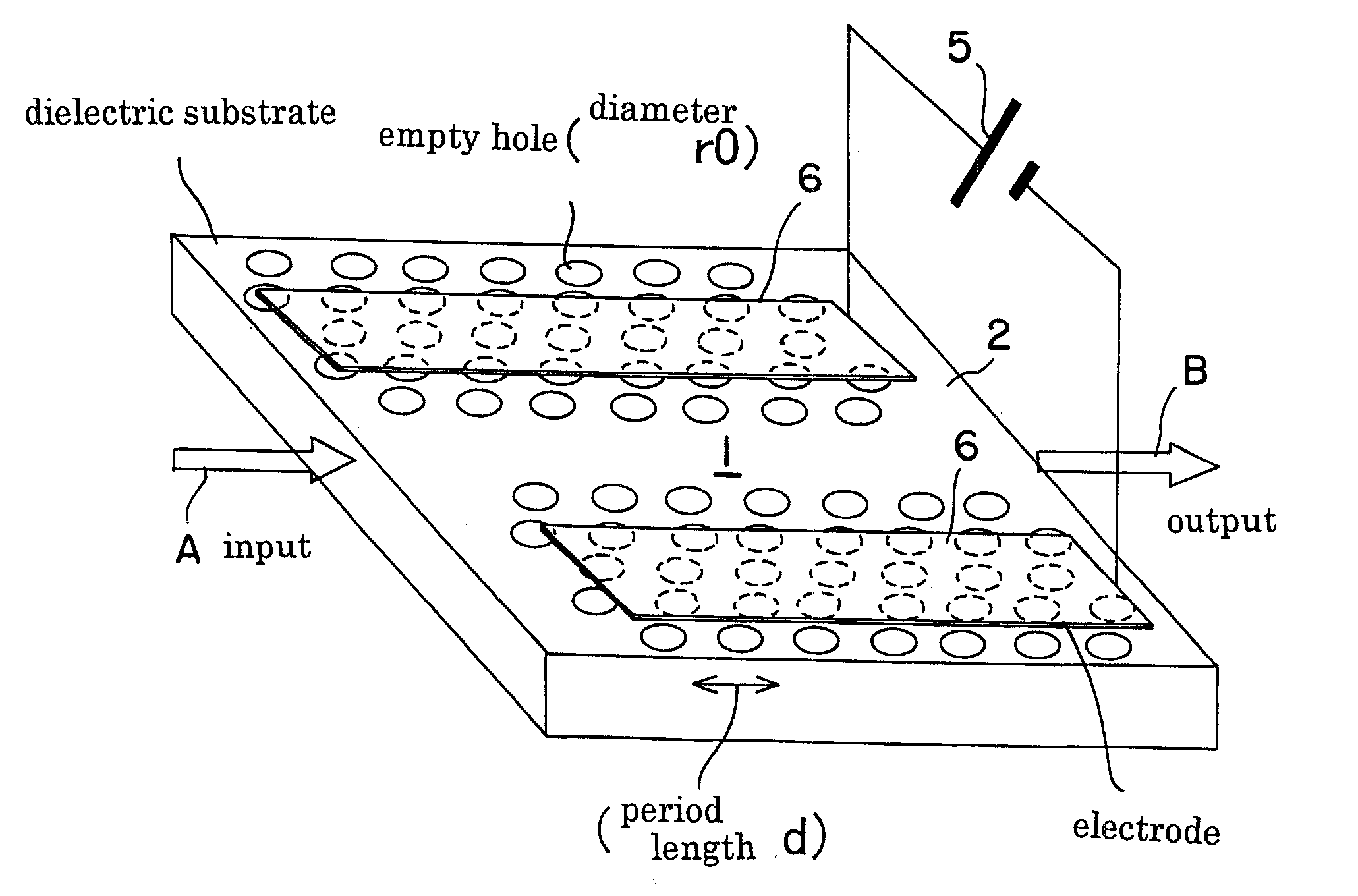
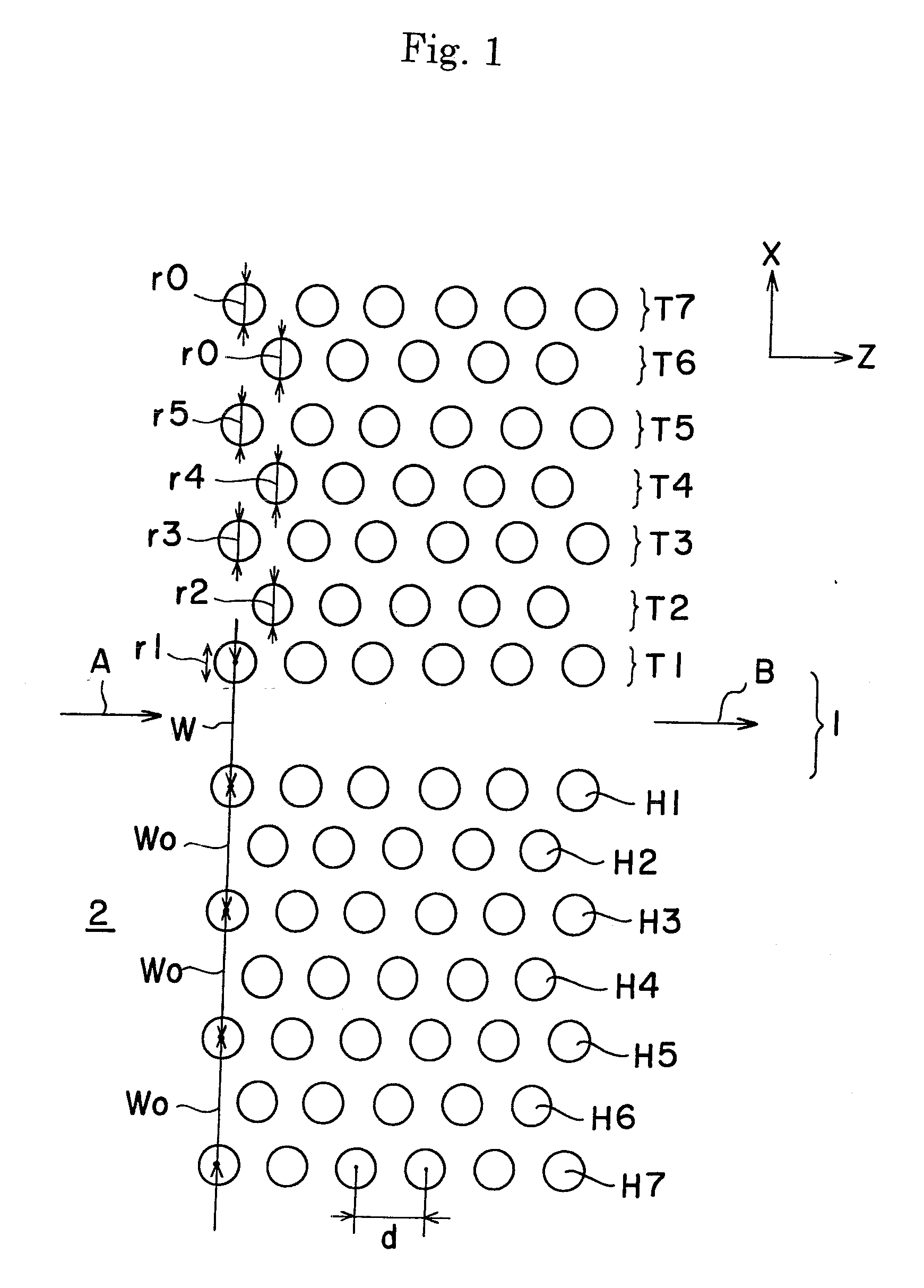
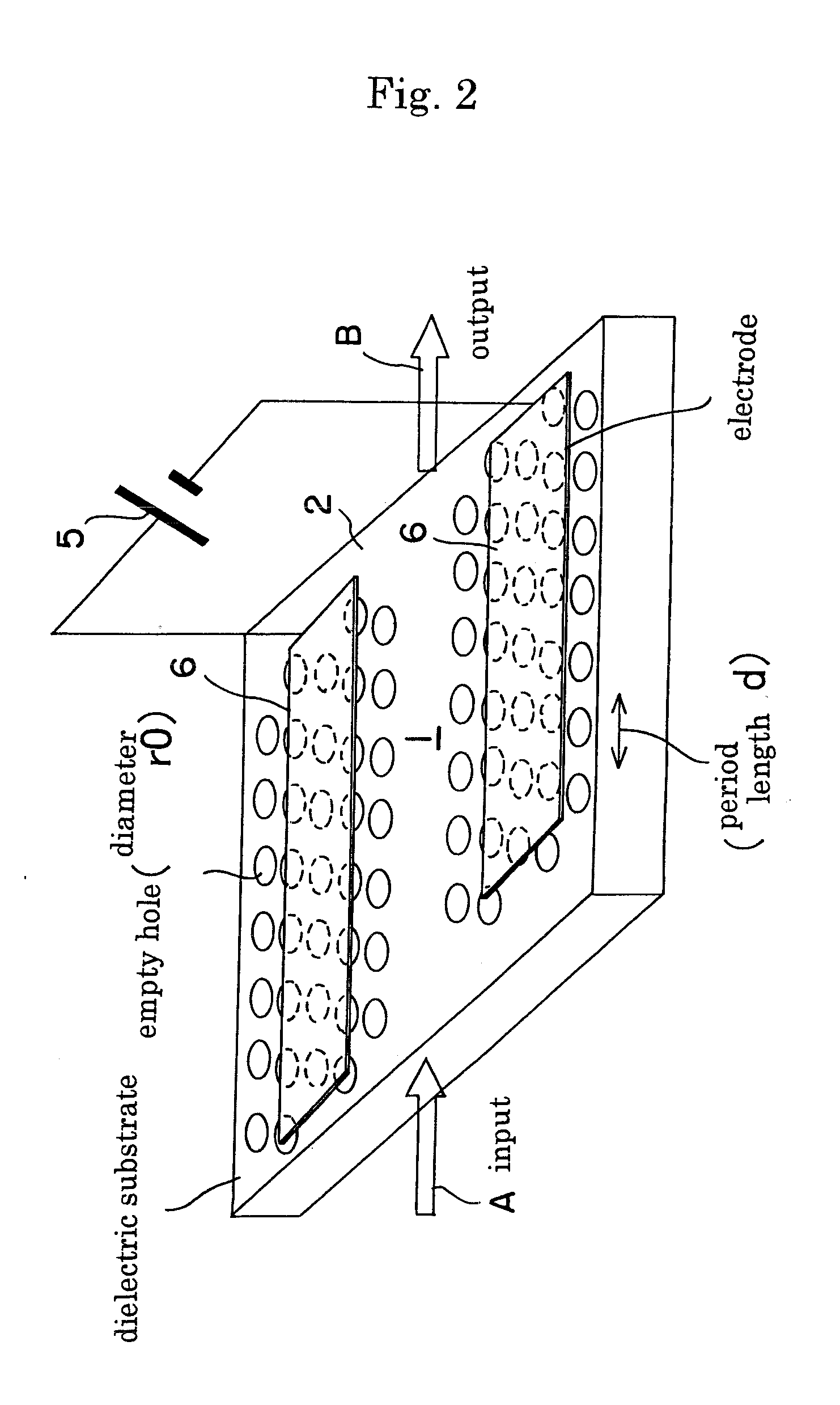
[0042]A photonic crystal is a multi-dimension and periodic structure having a periodicity comparable with a wavelength of light with a plurality of media having different refractive indices. The photonic crystal has a band structure of light similar to that of electron. Specific structure thus provides photonic band gap of light. The photonic crystal having the photonic band gap functions as an insulator of light.
[0043]Linear defects can be introduced into a photonic crystal having photonic band-gap for deteriorating its periodicity. It is thereby possible to form waveguide mode in a frequency region of the band-gap and to provide an optical waveguide confining light.
[0044]A slab-type two-dimensional photonic crystal defined as follows. That is, to a dielectric thin film slab, low dielectric pillars are provided at an appropriate two-dimensional period. Each dielectric pillar has a refractive index lower than that of the dielectric thin film slab and has a shape of a column or an eq...
PUM
 Abstract
Description
Claims
Application Information