Light emitting device package and lighting system

a technology of light emitting devices and lighting systems, applied in the direction of basic electric elements, semiconductor devices, electrical equipment, etc., can solve problems such as the reliability of wire bonding

Active Publication Date: 2012-06-21
SUZHOU LEKIN SEMICON CO LTD
View PDF17 Cites 10 Cited by
  • Summary
  • Abstract
  • Description
  • Claims
  • Application Information

AI Technical Summary

Problems solved by technology

If the LED is electrically connected to the lead frames th...

Method used


Image

  • Light emitting device package and lighting system
  • Light emitting device package and lighting system
  • Light emitting device package and lighting system

Examples


Embodiment Construction

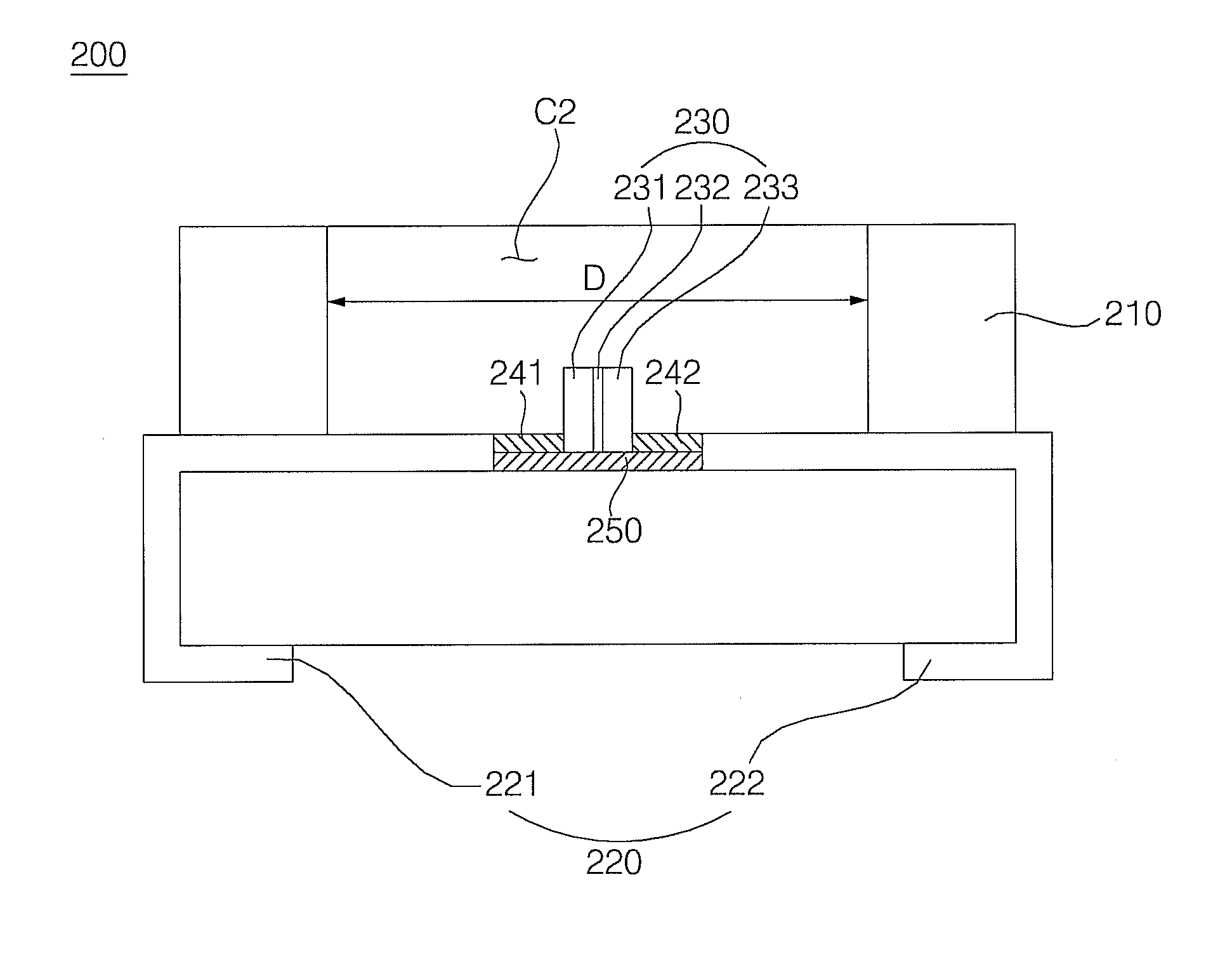
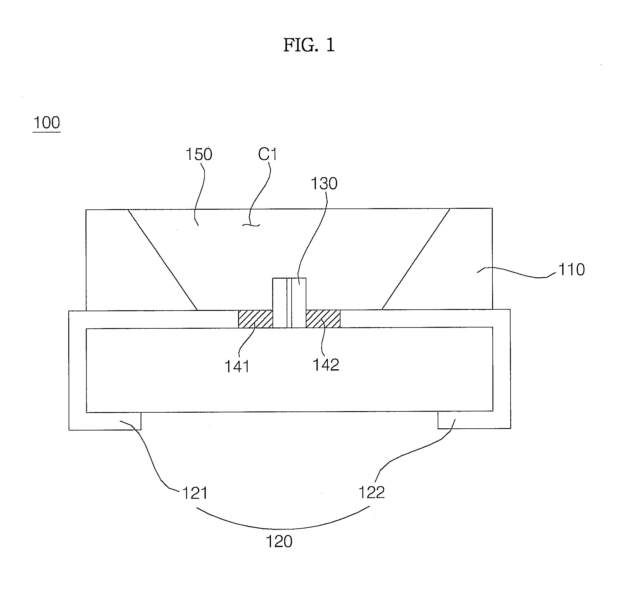
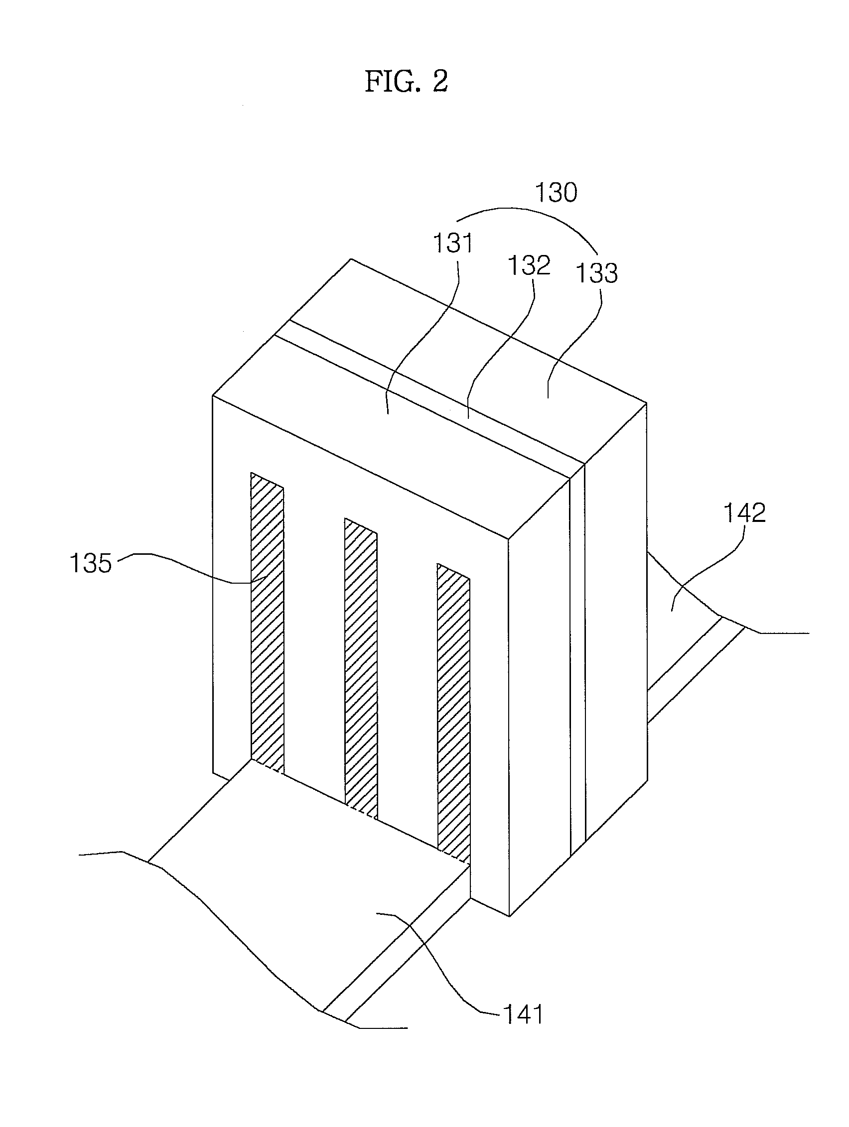
[0017]Reference will now be made in detail to embodiments, examples of which are illustrated in the accompanying drawings. However, the present disclosure may be embodied in many different forms and should not be construed as limited to the embodiments set forth herein. Rather, these embodiments are provided so that this disclosure will be thorough and complete, and will fully convey the scope of the disclosure to those skilled in the art. The present disclosure is defined only by the categories of the claims. In certain embodiments, detailed descriptions of device constructions or processes well known in the art may be omitted to avoid obscuring appreciation of the disclosure by a person of ordinary skill in the art. Wherever possible, the same reference numbers will be used throughout the drawings to refer to the same or like parts.

[0018]Spatially-relative terms such as “below”, “beneath”, “lower”, “above”, or “upper” may be used herein to describe one element's relationship to an...


PUM


Abstract

The light emitting device package includes a body provided with a cavity, a first lead frame mounted on the body, a second lead frame mounted on the body and separated from the first lead frame, and a light emitting device mounted in the cavity and disposed between the first lead frame and the second lead frame, the light emitting device is formed by sequentially stacking a first conductivity-type semiconductor layer, an active layer and a second conductivity-type semiconductor layer, the sequentially stacking direction of the first conductivity-type semiconductor layer, the active layer and the second conductivity-type semiconductor layer is parallel with the bottom surface of the cavity, the first lead frame includes a first connection part electrically connected to the first conductivity-type semiconductor layer, and the second lead frame includes a second connection part electrically connected to the second conductivity-type semiconductor layer.

Description

CROSS-REFERENCE TO RELATED APPLICATION[0001]This application claims the priority benefit of Korean Patent Application No. 10-2011-0075935, filed on Jul. 29, 2011 in the Korean Intellectual Property Office, the disclosure of which is incorporated herein by reference.BACKGROUND[0002]1. Field[0003]Embodiments relate to a light emitting device package, and more particularly to a light emitting device package in which a light emitting device is disposed between lead frames so as to omit wire bonding.[0004]2. Description of the Related Art[0005]Light emitting diodes (LEDs) are devices which convert an electrical signal into light using characteristics of a compound semiconductor, and are used in household electric appliances, remote controllers, electronic bulletin boards, displays, various automated machines, etc., and using fields of the LEDs are gradually increased.[0006]In general, a small LED is fabricated into a surface mount device type in order to be directly mounted on a printed ...

Claims


Application Information

Patent Timeline
IPC IPC(8): H01L33/60H01L33/48
CPCH01L33/38H01L33/60H01L33/62H01L33/486H01L2924/0002H01L2924/00H01L33/48H01L33/483
Inventor KONG, JIUNSEO, IL
Owner SUZHOU LEKIN SEMICON CO LTD
Why Eureka
Try Eureka