Supercharge Your Innovation With Domain-Expert AI Agents!

Dot inversion TFT array and LCD panel

a technology of tft array and display panel, applied in the field of thin film transistor array and associated display panel, can solve the problems of incompetence of art applied to a dual gate tft array in achieving complete dot inversion

Active Publication Date: 2012-07-12
MEDIATEK INC
View PDF3 Cites 7 Cited by
  • Summary
  • Abstract
  • Description
  • Claims
  • Application Information

AI Technical Summary

Benefits of technology

[0020]The invention is directed to a TFT array and associated control method, which displays an image with a dot inversion approach by implementing a dual gate TFT array driven by same gate driving signals and source driving signals.

Problems solved by technology

Due to the increase in the size of LCD panels, the number of data lines on a source driver also gets larger and larger.
Nevertheless, a driving method associated with the prior art applied to a dual gate TFT array is incompetent in achieving complete dot inversion.

Method used


Image

  • Dot inversion TFT array and LCD panel
  • Dot inversion TFT array and LCD panel
  • Dot inversion TFT array and LCD panel

Examples


Embodiment Construction

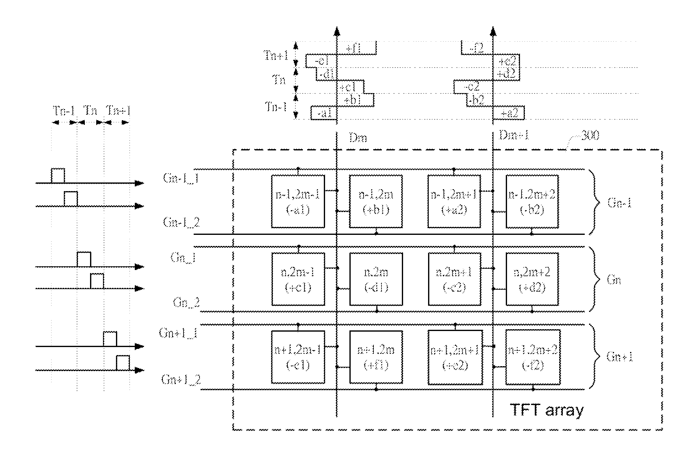
[0033]FIG. 4 shows a schematic diagram of a dual gate TFT array. A TFT array 300 comprises an (n−1)th gate line pair Gn−1, an nth gate line pair Gn, an (n+1)th gate line pair Gn+1, an mth data line Dm, and an (m+1)th data line Dm+1. The (n−1)th gate line pair Gn−1 controls (n−1, 2m−1) dot unit, an (n−1, 2m) dot unit, an (n−1, 2m+1) dot unit, and an (n−1, 2m+2) dot unit on an (n−1) row; the (n−1, 2m−1) dot unit and the (n−1, 2m) dot unit are connected to the data line Dm, and the (n−1, 2m+1) dot unit and the (n−1, 2m+2) dot unit are connected to the data line Dm+1. The gate line pair Gn controls an (n, 2m−1) dot unit, an (n, 2m) dot unit, an (n, 2m+1) dot unit, and an (n, 2m+2) dot unit on an nth row. The (n, 2m−1) dot unit and the (n, 2m) dot unit are connected to the data line Dm, and the (n, 2m+1) dot unit and the (n, 2m+2) dot unit are connected to the data line Dm+1. The gate line pair Gn+1 controls (n+1, 2m−1) dot unit, an (n+1, 2m) dot unit, an (n+1, 2m+1) dot unit, and an (n+...


PUM


Abstract

A dot inversion TFT array is provided. The dot inversion TFT array includes: a plurality of data lines; a plurality of dot unit pairs, each including a first dot unit and a second dot unit and coupled to one of the data lines; and a plurality of gate line pairs, each including a first gate line and a second gate line. A predetermined dot unit pair of the dot unit pairs is coupled to a predetermined gate line pair of the gate line pairs, and two horizontally neighboring dot unit pairs of the dot unit pairs are mirror-symmetrical.

Description

[0001]This application claims the benefit of Taiwan application Serial No. 100101016, filed Jan. 11, 2011, the subject matter of which is incorporated herein by reference.BACKGROUND OF THE INVENTION[0002]1. Field of the Invention[0003]The invention relates in general to a thin-film transistor (TFT) array and associated display panel, and more particularly to a dot inversion dual gate TFT array and associated LCD panel.[0004]2. Description of the Related Art[0005]FIG. 1 shows a schematic diagram of a conventional LCD panel. The LCD panel comprises a TFT array 100, a gate driver 120, a source driver 110, and a timing controller 130. The gate driver 120 and the source driver 110 control a plurality of dot units in the TFT array. The dot units are categorized into red dot units R, green dot units G, and blue dot units B. A combination of one red dot unit R, one green dot unit B, and one blue dot unit B forms a single pixel. The timing controller 130 generates a first timing control sign...

Claims


Application Information

Patent Timeline
Patent Type & Authority Applications(United States)
IPC IPC(8): G09G5/00G09G3/36
CPCG09G3/3614G09G2300/0426G09G3/3648
Inventor HSIEH, MIN-NANCHEN, JIAN-KAOLIN, CHIN-WEI
Owner MEDIATEK INC
Features
  • R&D
  • Intellectual Property
  • Life Sciences
  • Materials
  • Tech Scout
  • Unparalleled Data Quality
  • Higher Quality Content
  • 60% Fewer Hallucinations
Learn More