Semiconductor memory device

a memory device and semiconductor technology, applied in semiconductor devices, digital storage, instruments, etc., can solve the problems of increasing the leakage of cells caused by the fall of threshold voltage, the difficulty of securing a cell capacity or suppressing leakage current, and the likely large problem of power supply voltage falling

Inactive Publication Date: 2006-09-05
KK TOSHIBA
View PDF16 Cites 14 Cited by
  • Summary
  • Abstract
  • Description
  • Claims
  • Application Information

AI Technical Summary

Problems solved by technology

With further miniaturization in the future, however, the fall of power supply voltage will probably become a large problem in designing of a semiconductor memory.
However, for example, an increase of cell leakage caused by the fall of threshold voltage becomes a problem in a static random access memory (SRAM).
In the DRAM, the progress in miniaturization has brought about a difficulty of securing a cell capacity or suppressing leakage current.
Consequently, when the power supply voltage (high-level bit line voltage VBLH) is lowered, the amount of charges accumulated in the cell is reduced, deteriorating data saving performance.
In this case, however, a transition speed of the bit line pair BL, / BL becomes slow.
Thus, if the leakage causes a fall of the potential of the common source line to a certain level, before a sufficient signal is output from the cell to the bit line BL after the precharging of the BL is released, a sense operation is started (slowly), creating a possibility of an erroneous operation.
Arrangement of such a small precharge transistor for each column, or for some columns leads to low layout efficiency.
As described above, the power supply voltage of the memory cell portion will have to be set higher than that of the peripheral circuit portion (logic portion), making difficult the writing operation of the semiconductor memory in the future.
Under such circumstances, connecting of the sense amplifier circuits of all the columns and all the SA drivers in the SA bank to the common source line to achieve a high writing speed makes the writing operation more difficult.
Then, in reality, there will be no practical solutions.

Method used


Image

  • Semiconductor memory device
  • Semiconductor memory device
  • Semiconductor memory device

Examples


first embodiment

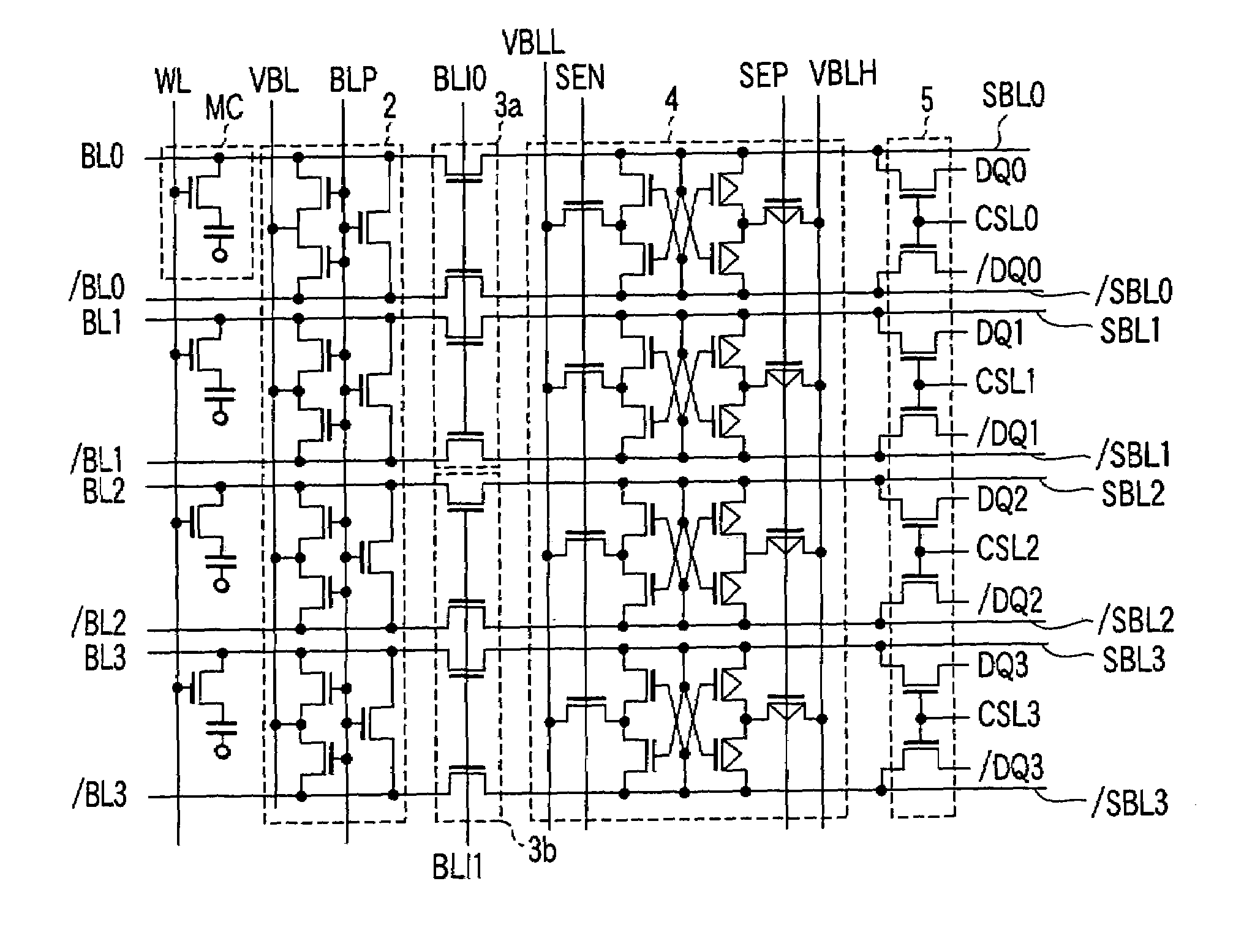
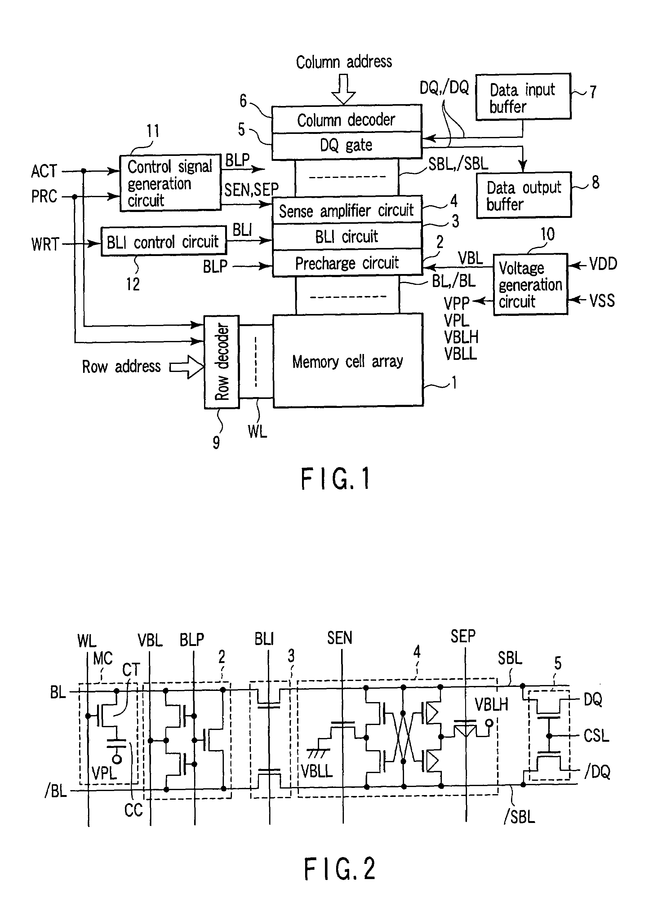
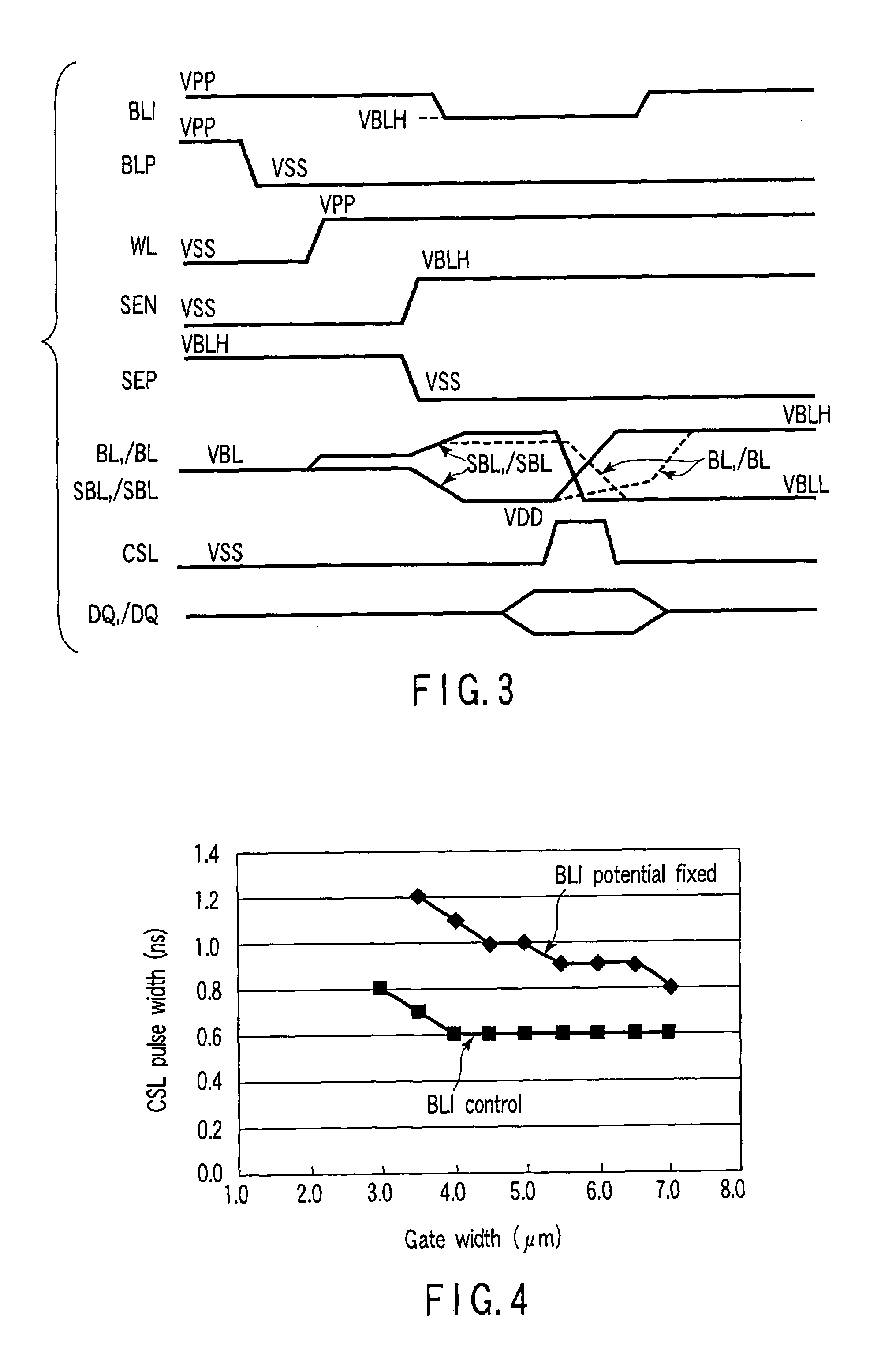
[0104]FIG. 1 is a block diagram showing a main portion of a semiconductor memory device according to a first embodiment of the invention. This semiconductor memory device comprises a memory core unit constituted of a memory cell array, a row decoder, a sense amplifier circuit, a precharge circuit and a bit line isolation (BLI) circuit, and another peripheral logic portion. Referring to FIG. 1, the memory cell array 1 is disposed by arranging memory cells MC in a matrix form. The precharge circuit 2 is connected to the memory cell array 1 via a bit line pair BL, / BL. The precharge circuit 2 precharges a bit line to a precharge voltage VBL.

[0105]A sense amplifier bit line pair SBL, / SBL is disposed corresponding to each bit line pair BL, / BL. The bit line pair BL, / BL and the bit line pair SBL, / SBL are interconnected by the bit line isolation (BLI) circuit 3. The sense amplifier circuit 4 is connected to the bit line pair SBL, / SBL. The sense amplifier circuit 4 amplifies data of the...

second embodiment

[0140]According to a second embodiment, a BLI circuit 3 comprises a transfer gate constituted of NMOS and PMOS transistors.

[0141]FIG. 5 is a circuit diagram of a semiconductor memory device according to the second embodiment of the invention. Referring to FIG. 5, the BLI circuit 3 comprises two transfer gates TG1, TG2. The transfer gates TG1, TG2 are configured by connecting NMOS and PMOS transistors in parallel.

[0142]A BLI control circuit 12 generates bit line isolation signals NBLI and PBLI for controlling resistance values of the transfer gates TG1, TG2. The signal NBLI is input to gates of the NMOS transistors of the transfer gates TG1, TG2. The signal PBLI is input to gates of the PMOS transistors of the transfer gates TG1, TG2. Other components are similar to those of FIG. 1, and thus a block diagram thereof will be omitted.

[0143]FIG. 6 is a timing chart of the semiconductor memory device shown in FIG. 5. The BLI control circuit 12 normally generates a bit line isolation signa...

third embodiment

[0157]FIG. 7 is a block diagram showing a main portion of a semiconductor device according to a third embodiment of the invention.

[0158]The semiconductor memory device comprises a CSL detection circuit 13. A column selection signal CSL generated by a column decoder 6 is input to the CSL detection circuit 13. The CSL detection circuit 13 detects timing of deactivating a signal CSL. In other words, it detects falling of the signal CSL. The CSL detection circuit 13 inputs a trigger signal CSLT to a BLI control circuit 12.

[0159]Upon reception of the signal CSLT from the CSL detection circuit 13, the BLI control circuit 12 returns a potential of the signal BLI from VBLH to VPP.

[0160]FIG. 8 is a timing chart of the semiconductor memory device shown in FIG. 7.

[0161]When the signal CSL is changed from a “L” level (VSS) to a “H” level (e.g., VDD), data of the bit line pair SBL, / SBL is reversed by data transferred from the data line pair DQ, / DQ, and the reversed data is held in the sense am...


PUM


Abstract

A semiconductor memory device includes a memory cell array which has a plurality of memory cells, a plurality of first bit line pairs which transfer data among the memory cells, a plurality of second bit line pairs disposed corresponding to the plurality of first bit line pairs, a plurality of variable resistance elements disposed to connect the plurality of first bit line pairs to the plurality of second bit line pairs, a plurality of data line pairs disposed corresponding to the plurality of second bit line pairs, a plurality of input / output gates which transfer data between the plurality of second bit line pairs and the plurality of data line pairs, a plurality of sense amplifier circuits which amplify data transferred to the plurality of second bit line pairs, and a bit line isolation control circuit which controls resistance values of the plurality of variable resistance elements.

Description

CROSS-REFERENCE TO RELATED APPLICATIONS[0001]This application is based upon and claims the benefit of priority from prior Japanese Patent Applications No. 2004-115700, filed Apr. 9, 2004; and No. 2005-014180, filed Jan. 21, 2005, the entire contents of both of which are incorporated herein by reference.BACKGROUND OF THE INVENTION[0002]1. Field of the Invention[0003]The present invention relates to a semiconductor memory device, and more particularly to a semiconductor memory device which comprises a circuit for writing data to a memory cell.[0004]2. Description of the Related Art[0005]A writing operation of a conventional semiconductor memory device such as a dynamic random access memory (DRAM) will be described. FIG. 57 is a circuit diagram showing a part of a DRAM configuration. This DRAM comprises a memory cell array in which memory cells MC are arranged in a matrix form, a plurality of bit line pairs BL, / BL, a plurality of word lines, a precharge circuit 2, a sense amplifier ci...

Claims


Application Information

Patent Timeline
Patent Type & Authority Patents(United States)
IPC IPC(8): G11C7/00G11C7/02H01L27/10G11C7/12G11C8/00G11C11/401G11C11/409G11C11/4094H01L21/8242H01L27/108
CPCG11C7/08G11C7/18G11C7/22G11C11/4074G11C11/4076G11C11/4085G11C11/4091G11C11/4094G11C11/4097G11C29/50008G11C7/12H01L27/10897G11C2207/002G11C2207/005G11C2207/065G11C2207/2281G11C2207/229H01L27/0207H10B12/50
Inventor KAJITANI, YASUYUKIKATO, DAISUKE
Owner KK TOSHIBA
Why Eureka
Try Eureka