

Process of Multiple Exposures With Spin Castable Films
a castable film and multiple exposure technology, applied in the field of semiconductor devices, can solve the problems of limiting the pitch and/or resolution of printed images for certain applications such as contacts, using conventional single-layer resists in integrated circuitry fabrication, and limiting the pitch and/or resolution of printed images for certain applications, etc., to achieve cost-effective, high-resolution patterning techniques, and cost-saving effects
- Summary
- Abstract
- Description
- Claims
- Application Information
AI Technical Summary
Benefits of technology
Problems solved by technology
Method used
Image

Examples
Embodiment Construction
[0001]1. Field of the Invention
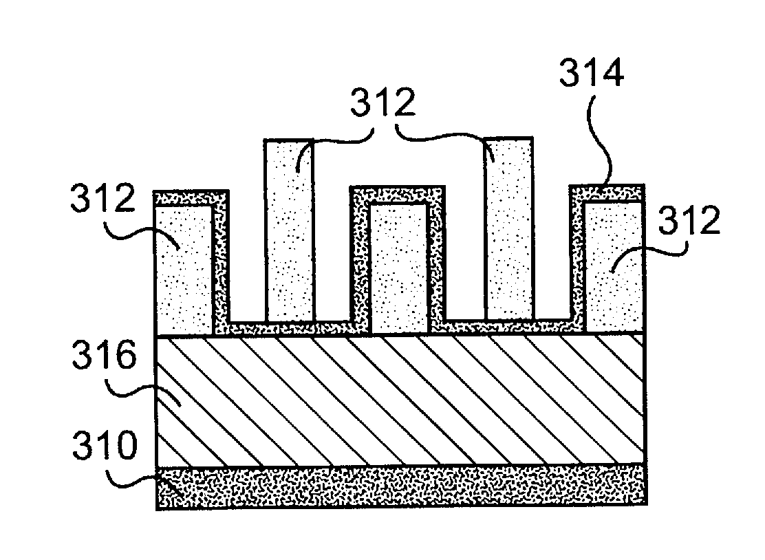
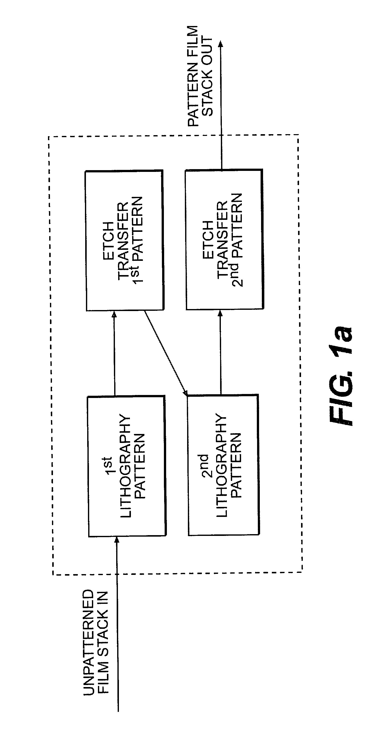
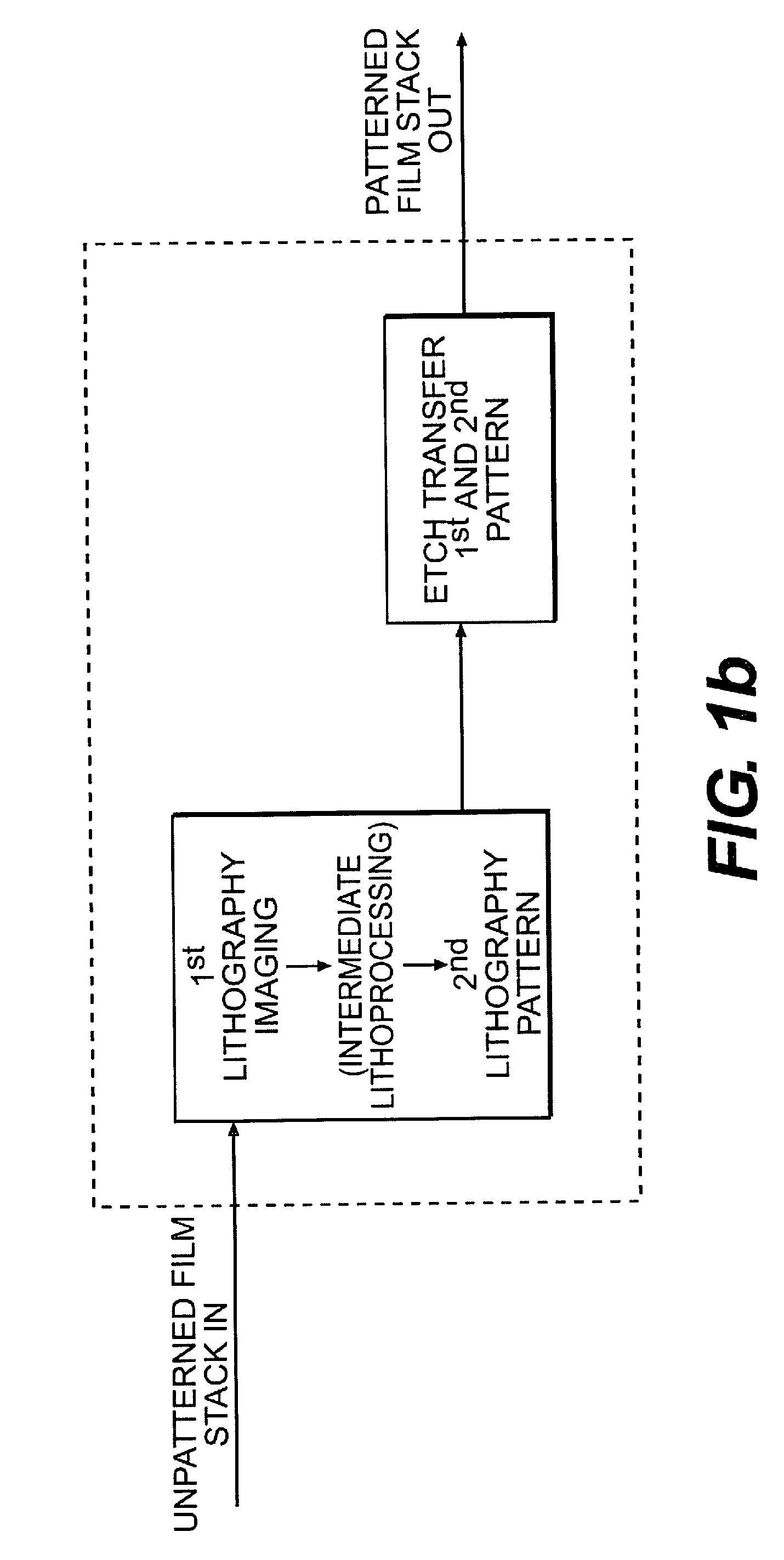
[0002]The field of the invention comprises semiconductor devices, and a process for producing semiconductor devices by techniques that embody semiconductor device resolution enhancement through multiple exposure lithography incorporating intermediate layer patterning.
[0003]2. Background of the Invention
[0004]Lithography is one of the most important techniques utilized in semiconductor manufacturing, and is particularly used to define patterns, as for example those employed in a wiring layer patterning process, a device width defining process, or a doped-region defining process. A lithography process generally includes an exposure step and a development step, wherein the exposure step utilizes a light source to irradiate a photoresist layer directly or through a photo mask to induce chemical reactions in exposed portions. The development step is conducted to remove the exposed portion in positive resist (or the unexposed portion in negative resist) and ...
PUM
 Abstract
Description
Claims
Application Information