Image Pickup Device and Method for Manufacturing the Image Pickup Device
a pickup device and image technology, applied in the field of image pickup devices, can solve the problems of reducing productivity, difficult to cut precisely enough to maintain high optical performance, deteriorating the cutting blade for dicing, etc., and achieves the effects of high productivity, improved cutting resistance, and improved cutting resistance when cutting
- Summary
- Abstract
- Description
- Claims
- Application Information
AI Technical Summary
Benefits of technology
Problems solved by technology
Method used
Image
Examples
first embodiment
[0144][Image Pickup Device]
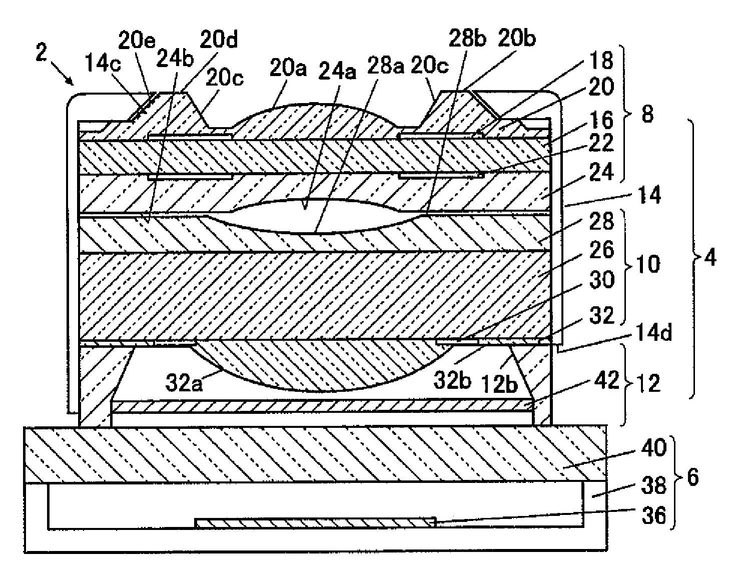
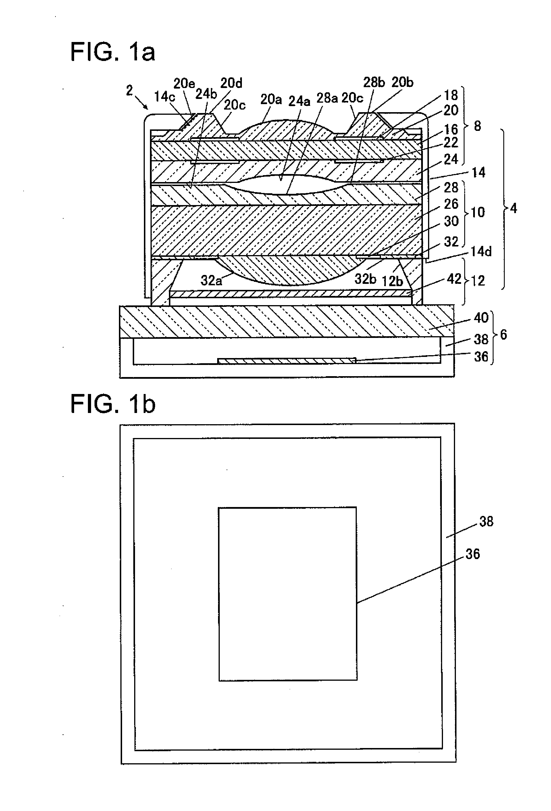
[0145]As shown in FIG. 1a, an image pickup device 2 is mainly constituted by a lens unit 4 and a sensor unit 6, and the lens unit 4 is disposed on the sensor unit 6. The sensor unit 6 has a larger area than the lens unit 4, and thus the lens unit 4 is mounted on the center of the sensor unit 6 with an open area (forming a step) on the circumference of the sensor unit 6.
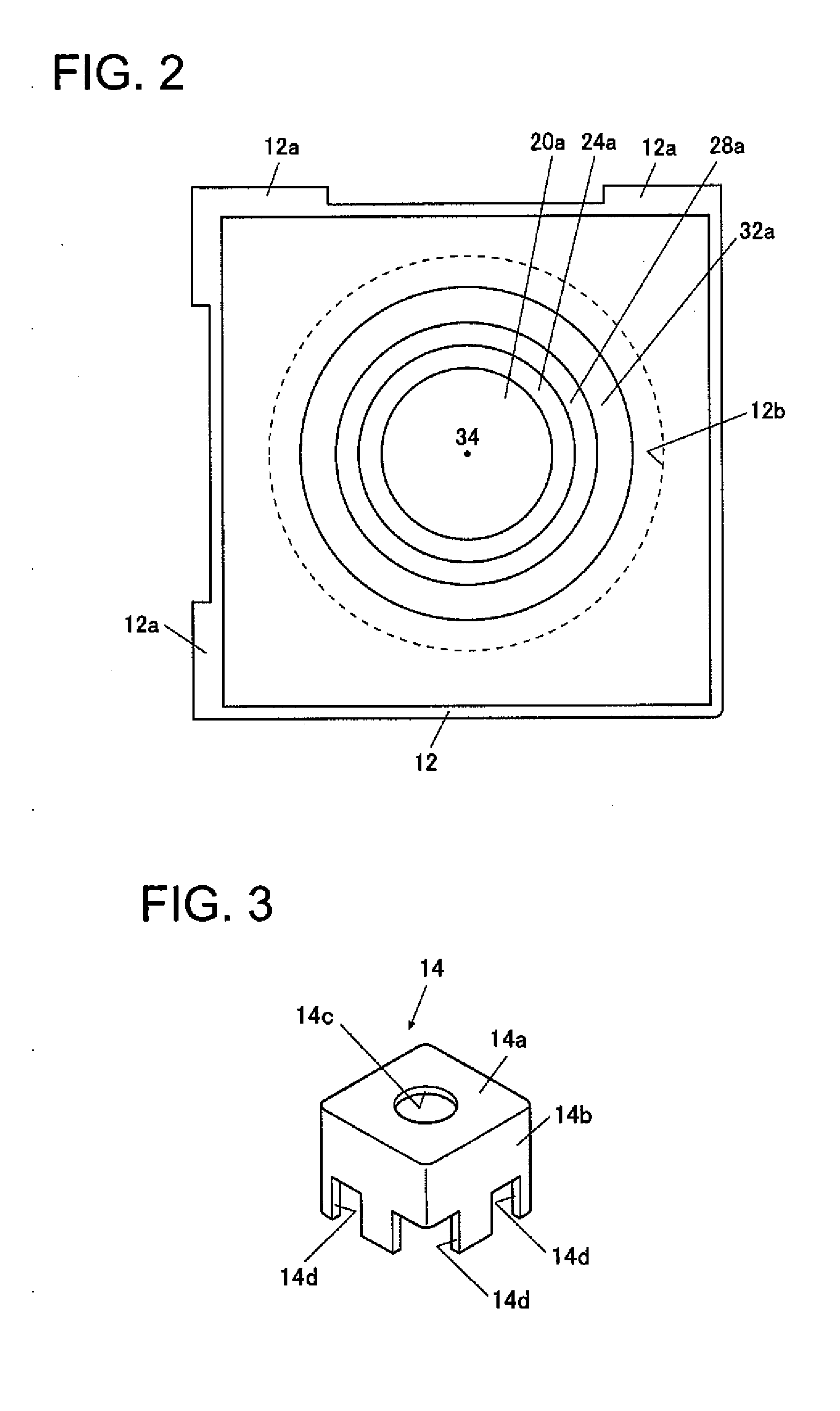
[0146]The lens unit 4 includes: a lens block 8 in which a convex lens part 20a, a glass substrate 16, and a concave lens part 24a are bonded together; a lens block 10 in which a concave lens part 28a, a glass substrate 26, and a convex lens part 32a are bonded together; a spacer 12; and a covering package 14, wherein the lens blocks 8 and 10 and the spacer 12 are stacked and bonded and covered by a covering package 14.
[0147]The lens block 8 has a plate-like glass substrate 16. On the glass substrate 16, there are formed an aperture stop 18 and a resin part 20, and under the glass substrate 1...
second embodiment
[0569]The second embodiment is different from the first embodiment mainly on the following points, but the same as the first embodiment on the other points.
[0570]As a wafer lens manufacturing apparatus, instead of the wafer lens manufacturing apparatus 300, a wafer lens manufacturing apparatus 700 is used.
[0571]In producing the wafer lens 52 or 54, instead of a so-called step-and-repeat method (a method in which a molding die 450 is relatively moved to produce convex lens parts 20a and the like, gradually), a so-called batch method (a method in which a molding die 770 is pressed on a glass substrates 16 and 26 once to collectively produce the convex lens parts 20a and the like) is employed.
[0572][Wafer Lens Manufacturing Apparatus (Batch Method)]
[0573]As shown in FIG. 68, the wafer lens manufacturing apparatus 700 has a base 702.
[0574]On the upper part of the base 702, there is formed an opening section 704. Over the opening section 704, there is provided a plate-like lid body 706 d...
PUM
 Abstract
Description
Claims
Application Information


