Oxide semiconductor device including insulating layer and display apparatus using the same

a technology of insulating layer and display apparatus, which is applied in the direction of semiconductor devices, electrical apparatus, transistors, etc., can solve the problems of difficult application of this method to plastic substrates or the like with low heat resistance, the display apparatus using the oxide semiconductor device manufactured by the low temperature process cannot achieve the practical use, and the resistance of the semiconductor layer is reduced. , to achieve the effect of high productivity and lowering the resistance of the semiconductor layer

Active Publication Date: 2010-11-11
CANON KK
View PDF17 Cites 269 Cited by
  • Summary
  • Abstract
  • Description
  • Claims
  • Application Information

AI Technical Summary

Benefits of technology

[0021]According to the present invention, lowering of the resistance of the semiconductor layer, which is caused by water in the atmosphere, hydrogen diffused from the barrier layer (from the barrier coating layer and the protective layer), and water or hydrogen diffused from the substrate, can be effectively suppressed. Further, there can be provided an oxide semiconductor device which can be formed at a temperature of 250° C. or less by the low temperature process using the barrier layer containing hydrogen at more than 4×10²¹ atoms / cm3 and which has high productivity. Besides, PECVD can be used as a formation method for the barrier layer.

Problems solved by technology

Moreover, it is known that, in an oxide semiconductor device using ZnO as a main component, when silicon nitride (SiNx) formed by plasma enhanced chemical vapor deposition (also referred to as PECVD) is used as a gate insulating layer, the following problem occurs.
However, it is difficult to apply this method to a plastic substrate or the like with low heat resistance, because the substrate itself does not have sufficient heat resistance to a manufacturing temperature or an anneal temperature for the oxide semiconductor.
However, an insulating layer functioning as the barrier layer such as the barrier coating layer or the protective layer, which is formed by PECVD, contains a large amount of in-film hydrogen (amount of hydrogen contained in the insulating layer), and hence the oxide semiconductor cannot be formed without making the oxide semiconductor have lower resistance.
Therefore, a display apparatus using the oxide semiconductor device manufactured by the low temperature process has not achieved its practical use.

Method used


Image

  • Oxide semiconductor device including insulating layer and display apparatus using the same
  • Oxide semiconductor device including insulating layer and display apparatus using the same
  • Oxide semiconductor device including insulating layer and display apparatus using the same

Examples


example 1

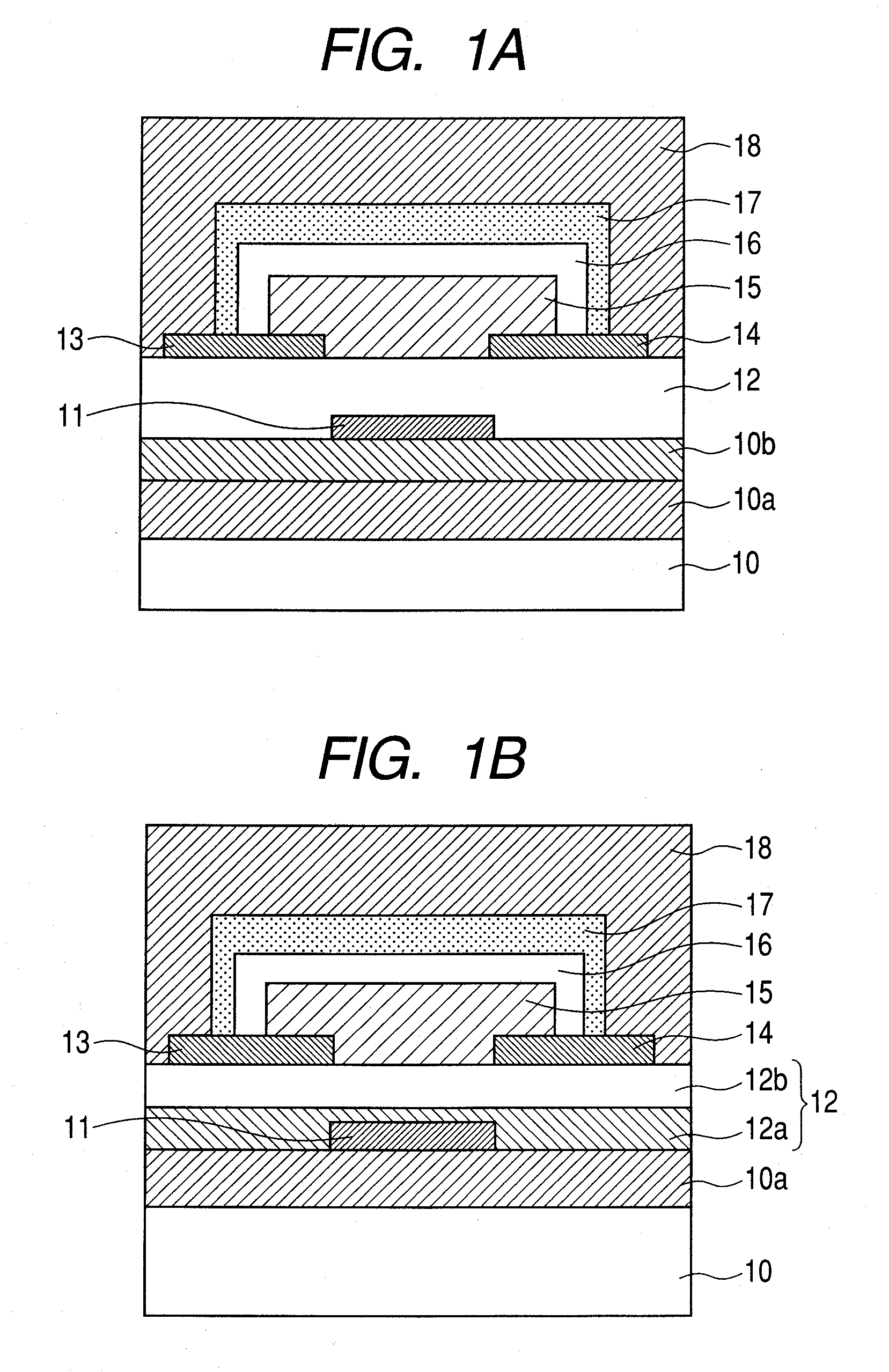
Bottom-Gate / Bottom-Contact Field Effect Transistor

[0105]An example in which the bottom-gate / bottom-contact field effect transistor of FIG. 9 is manufactured is described. First, an electrode layer for forming a gate electrode is formed on the glass substrate 10 (manufactured by Corning Inc., #1737) by sputtering. The electrode is formed of Mo and has a thickness of 50 nm.

[0106]Then, the electrode is patterned by photolithography and etching to form the gate electrode 11.

[0107]Next, an SiOx film is formed with a thickness of 200 nm by sputtering to serve as the gate insulating layer 12. The SiOx film is formed with a radio frequency (RF) sputtering apparatus at a substrate temperature of room temperature. A target is SiO2 with a diameter of 3 inches. The RF input power is 400 W. The total pressure of the atmosphere at the film formation is 0.5 Pa, and the gas flow rate at that time is Ar=100%. The source electrode 13 and the drain electrode 14 are formed of indium tin oxide (ITO) and...

example 2

[0109]An example in which the bottom-gate / top-contact field effect transistor of FIG. 12D is manufactured is described.

[0110]First, on the glass substrate 10 containing an alkali metal, the barrier coating layer 10a is formed of SiNz at a temperature of 250° C. by PECVD. Thereon, the gate electrode 11 is patterned by using photolithography, lift-off, and electron-beam evaporation. The gate electrode 11 is a laminated layer of Ti of 5 nm / Au of 40 nm / Ti of 5 nm, which is deposited on the barrier coating layer 10a by electron-beam evaporation.

[0111]Next, the laminated structure of the gate insulating layer 12a formed of SiNy and the gate insulating layer 12b formed of SiOx is used, and SiNy with a thickness of 150 nm and SiOx with a thickness of 50 nm are sequentially deposited, respectively, at room temperature (25° C.) by sputtering as in Example 1. The gate insulating layer 12b functions as the underlying layer of the oxide semiconductor layer 15. The oxide semiconductor layer 15 is...

example 3

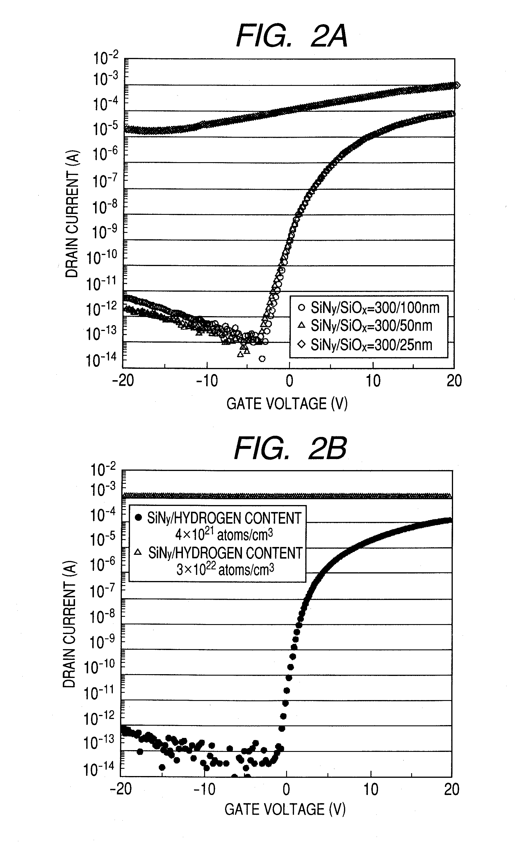
[0117]This example is an example in which the barrier coating layer 10a of Example 2 is formed of SiOmNn at the substrate temperature of 250° C. by PECVD. When the SiOmNn is formed, the substrate temperature is set to 250° C. As process gases, an SiH4 gas, an N2O gas, and an N2 gas are used. The gas flow rate is set to SiH4:N2O:N2=1:2.5:10. An RF input power density and a pressure are set to 0.25 W / cm2 and 150 Pa, respectively. Instead of the N2 gas, an NH3 gas may be used. After the barrier coating layer 10a is formed, other components are formed in the same manner as in Example 2. Thus, the bottom-gate / top-contact field effect transistor of the present invention is completed.

[0118]The bottom-gate / top-contact field effect transistor manufactured according to this example exhibits excellent characteristics with regard to hysteresis characteristics, uniformity, high-speed operability, and the like.


PUM


Abstract

Provided is an oxide semiconductor device including an oxide semiconductor layer and an insulating layer coming into contact with the oxide semiconductor layer in which the insulating layer includes: a first insulating layer coming into contact with an oxide semiconductor, having a thickness of 50 nm or more, and including an oxide containing Si and O; a second insulating layer coming into contact with the first insulating layer, having a thickness of 50 nm or more, and including a nitride containing Si and N; and a third insulating layer coming into contact with the second insulating layer, the first insulating layer and the second insulating layer having hydrogen contents of 4×10²¹ atoms / cm3 or less, and the third insulating layer having a hydrogen content of more than 4×10²¹ atoms / cm3.

Description

TECHNICAL FIELD[0001]The present invention relates to an oxide semiconductor device. More particularly, the present invention relates to an oxide semiconductor device including an insulating layer and to a display apparatus which is an application example of the oxide semiconductor device.BACKGROUND ART[0002]In recent years, thin film transistors (TFTs) including a channel layer of a transparent conductive oxide polycrystalline thin film containing zinc oxide (ZnO) as a main component have actively been developed (Japanese Patent Application Laid-Open No. 2002-076356).[0003]The transparent conductive oxide polycrystalline thin film can be formed at low temperature and is transparent with respect to a visible light, and hence a flexible transparent TFT can be formed on a substrate such as a plastic plate or a film.[0004]However, an oxide semiconductor containing ZnO has high sensitivity with respect to an atmosphere, and hence, in order to put the oxide semiconductor into practical u...

Claims


Application Information

Patent Timeline
Patent Type & Authority Applications(United States)
IPC IPC(8): H01L33/00H01L29/02H01L29/786
CPCH01L29/78606H01L29/4908H01L29/7869
Inventor SATO, AYUMUHAYASHI, RYOYABUTA, HISATOWATANABE, TOMOHIRO
Owner CANON KK
Why Eureka
Try Eureka