Substrate processing apparatus

a processing apparatus and substrate technology, applied in the direction of coatings, heating element materials, chemical vapor deposition coatings, etc., can solve the problems of large gate leakage current, increased tunneling current, and unsuitability for base oxide films, so as to prevent contamination, suppress the warping of the substrate, and uniform temperature distribution of the substra

Active Publication Date: 2006-03-09
TOKYO ELECTRON LTD
View PDF13 Cites 259 Cited by
  • Summary
  • Abstract
  • Description
  • Claims
  • Application Information

AI Technical Summary

Benefits of technology

[0021] According to the present invention, a heater portion for heating a substrate introduced in a processing space is configured having a heating element contained inside a transparent case formed of quartz; thereby preventing contamination by employing the heating element, maintaining a uniform temperature distribution for the substrate, suppressing warping of the substrate, and enabling reliable and efficient deposition of the substrate. Accordingly productivity can be improved.
[0022] Furthermore, according to the present invention, an internal space of the processing vessel and an internal space of the transparent case are depressurized at the same time; thereby suppressing internal / external pressure of the transparent case and improving thermal conductivity of heat from the heating element by allowing the thickness of the transparent case to be thinner to the extent of the amount of reduced pressure upon the transparent case.
[0023] Furthermore, according to the present invention, a heating plate of SiC for being heated by the heating element is provided on the upper face of the transparent case such that the upper face of the heating plate is in the vicinity of and opposite to the bottom face of the substrate held by a holding member; thereby enabling improvement of thermal conductivity, heating of the substrate to a temperature of 700° C., and preventing cracking of the heating element by reducing difference of temperature of the heating element.
[0024] Furthermore, according to the present invention, the heating element, which includes a first SiC heating part or second and third SiC heating parts, is able to reliably perform heating without warping the peripheral part of the substrate by selectively switching the supply of power to the first SiC heating part, to either one of the second and third SiC heating parts, or to both.
[0025] Furthermore, according to the present invention, the entire face of the substrate can be efficiently and uniformly heated by providing a heat reflecting member below the heating element.

Problems solved by technology

In such an extremely thin gate insulation film, however, there inevitably arises a problem of increased tunneling current, while such an increased tunneling current causes the problem of large gate leakage current.
However, such a thermal oxide film formed at low temperature tends to contain a large amount of surface states and is not suitable for the base oxide film of a high-K dielectric gate oxide film.
However, it has been extremely difficult to form the base oxide film 12 with the thickness of 1 nm or less, such as 0.8 nm or less, or even approximately 0.4 nm corresponding to a thickness of 2-3 atomic layers, while simultaneously maintaining uniformity and reproducibility.
Such a problem of increase of the base oxide film 12 with thermal annealing process becomes a particularly serious problem in the case the thickness of the base oxide film 12 is reduced to several atomic layers or less.

Method used


Image

  • Substrate processing apparatus
  • Substrate processing apparatus
  • Substrate processing apparatus

Examples


Embodiment Construction

[0114] In the following, preferred embodiments of the present invention are described with reference to the accompanying drawings,

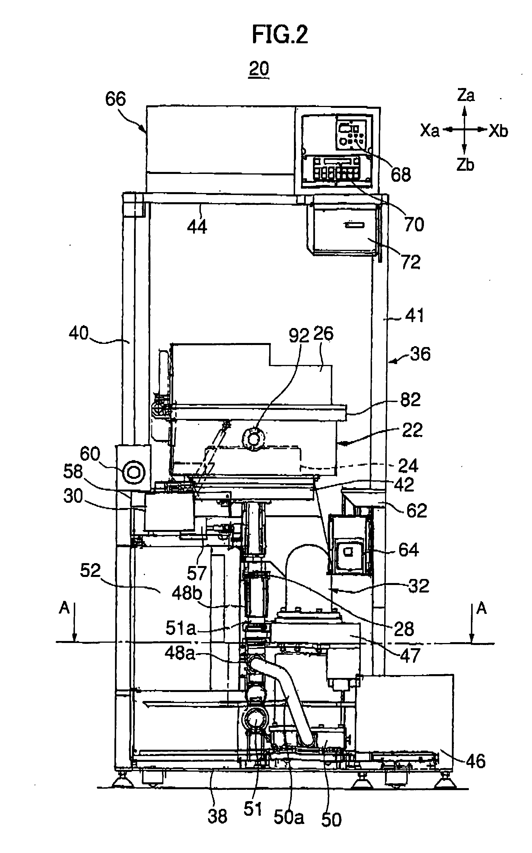
[0115]FIG. 2 is a front elevation view of a substrate processing apparatus according to an embodiment of the present invention. FIG. 3 is a side view of the substrate processing apparatus according to the present embodiment. FIG. 4 is a cross-sectional view of the substrate processing apparatus of FIG. 2 across line A-A.

[0116] The substrate processing apparatus 20 shown in FIGS. 2˜4 is configured to successively conduct a radical oxidation process using ultraviolet light on a silicon substrate and a radical nitridation process using a high frequency remote plasma of the oxide film formed by the radical oxidation process using ultraviolet light.

[0117] The substrate processing apparatus 20 includes a processing vessel 22 that defines a processing space, a heater portion 24 that is configured to heat a substrate (silicon substrate) introduced inside the p...


PUM

PropertyMeasurementUnit
gate lengthaaaaaaaaaa
thicknessaaaaaaaaaa
temperatureaaaaaaaaaa

Abstract

The substrate processing apparatus according to the present invention is aimed to stably and efficiently perform a deposition process on a substrate W. The substrate processing apparatus supports the substrate W in a position facing a heater portion and thus rotates a holding member holding the substrate W. Furthermore, the heating portion houses a SiC heater and a heat reflecting member in an internal portion of a quartz bell jar made of transparent quartz, and depressurizes an internal space of a processing vessel and an internal space of the quartz bell jar at the same time; thereby allowing the thickness of the quartz bell jar to be thinner, and thus improving thermal conductivity of heat from the SiC heater and preventing contamination by the SiC heater.

Description

TECHNICAL FIELD [0001] The present invention relates to a substrate processing apparatus and more particularly to a substrate processing apparatus that conducts processes such as a film forming process on a substrate. BACKGROUND ART [0002] In the technology of recent advanced high-speed semiconductor devices, use of the gate length of 0.1 μm or less is becoming possible with the progress in the art of ultrafine semiconductor fabrication processes. Generally, operational speed of a semiconductor device is improved with device miniaturization, while there is a need, in such extremely miniaturized semiconductor devices, to reduce the thickness of the gate insulation film thereof with the decrease of the gate length achieved as a result of the device miniaturization. [0003] When the gate length has been reduced to 0.1 μm or less, on the other hand, the thickness of the gate insulation film has to be reduced to 1-2 nm or less when a conventional thermal oxide film is used for the gate in...

Claims


Application Information

Patent Timeline
Patent Type & Authority Applications(United States)
IPC IPC(8): C23F1/00C23C16/00H05B3/14C23C16/46C23C16/48H01L21/00H01L21/31H01L21/316
CPCH01L21/67103C23C16/481C23C16/4586H01L21/68785H01L21/67109
Inventor HORIGUCHI, TAKAHIROKUWAJIMA, RYO
Owner TOKYO ELECTRON LTD
Why Eureka
Try Eureka