Process for production of semiconductor substrate

a technology of semiconductor substrates and processing methods, applied in semiconductor devices, semiconductor/solid-state device details, electrical devices, etc., can solve the problems of difficult formation of large-area substrates, limited application fields of soi techniques, and high cost of soi techniques, so as to achieve high quality, lower cost, and high productivity.

Inactive Publication Date: 2006-12-12
CANON KK
View PDF84 Cites 251 Cited by
  • Summary
  • Abstract
  • Description
  • Claims
  • Application Information

AI Technical Summary

Benefits of technology

[0035]In the present invention, the lamination-bonded substrates are separated at the porous layer, and the porous layer is removed from the second substrate having a nonporous monocrystalline semiconductor layer. Thereby, a semiconductor substrate is prepared which has nonporous monocrystalline semiconductor layer of high quality. Furthermore, the first substrate can be repeatedly used for producing the semiconductor substrate in the next production cycle by removing the remaining porous layer on the first substrate after the separation of the two substrate. Thereby, the semiconductor substrate can be produced with higher productivity and lower cost.
[0036]The present invention enables preparation of a monocrystalline layer of Si or the like, or a monocrystalline compound semiconductor layer having excellent crystallinity similar to monocrystalline wafers on a substrate including a light-transmissive substrate with advantages in productivity, uniformity, controllability, an production cost.
[0037]The present invention further enables production of a semiconductor substrate which can be a substitute for expensive SOS and SIMOX in production of large scale integrated circuits of an SOI structure.

Problems solved by technology

The SOS technique, which is successful as one of the SOI techniques, is limited in the application fields, because of many crystal defects caused by mismatch of the lattice at the interface between the Si layer and the underlying sapphire, contamination of the Si layer with aluminum from the sapphire substrate, expensiveness of the substrate, and difficulty of large-area substrate formation.
The compound semiconductor substrate, however, has disadvantages of high cost, low mechanical strength, and difficulty in formation of a large-area wafer.
These methods respectively have advantages and disadvantages, involving problems in process controllability, productivity, product uniformity, and product quality, and are not industrialized yet.
The beam annealing method involves problems in processing time of focused beam scanning and in controllability of beam superposition and focusing.
This method, however, still causes crystal defects in sub-grain boundaries, not being successful in production of a minority carrier device.
1. An oxidation film is formed on a monocrystalline Si substrate which has V-shaped grooves on the surface formed by anisotropical etching; a polycrystalline Si layer is deposited in a thickness approximate to that of the Si substrate on the oxidation film; and the back face of the Si substrate is ground to form a monocrystalline Si region isolated dielectrically by surrounding with the V-shaped grooves. This method involves problems in controllability and productivity in deposition of polycrystalline Si in a thickness of as large as several hundred microns, and in removal of the monocrystalline Si substrate by grinding at the back face to leave an isolated active Si layer only.
2. An SiO2 layer is formed by ion implantation into a monocrystalline Si substrate (SIMOX: Separation by ion implanted oxygen). This is the most highly advanced method in view of the matching with the Si process. This method, however, requires implantation of oxygen ions in an amount of as much as 1018 ions / cm2, which takes a long time, resulting in low productivity and high wafer cost. Further, the product has many remaining crystal defects, and does not have satisfactory properties for industrial production of a minority carrier device.
3. An SOI structure is formed by oxidation of porous Si for dielectric isolation. In this method, an N-type Si layer is formed in an island-like pattern on a P-type monocrystalline Si substrate surface by proton ion implantation (Imai, et al.: J. Crystal Growth, Vol. 63, p. 547 (1983)) or by epitaxial growth and patterning, and subsequently only the P-type Si substrate is made porous by anodic oxidation in an HF solution to surround the island-patterned N-type Si, and the N-type Si island is dielectrically isolated by accelerated oxidation. In this method, the isolated Si regions are fixed prior to the device process, which may limit the freedom of device design disadvantageously.
4. Differently from the above conventional SOI formation, a method has recently come to be noticed in which a monocrystalline Si substrate is bonded to another thermally oxidized monocrystalline Si substrate by heat treatment or use of an adhesive to form an SOI structure. This method requires uniform thinness of the active layer for the device: namely, formation of a film of a micron thick or thinner from a monocrystalline substrate of several hundred micron thick. This thin film may be formed by either of the two methods below.
1. Thin film formation by grinding, and
2. Thin film formation by selective etching.
The grinding method of “1” does not give readily a uniform thin film.
This irregularity is a serious problem.
With a larger diameter of the wafer, the uniformity of the thickness is much more difficult to attain.
This method, however, involves the problems of insufficient selectivity of about 102 at the highest, inferior surface properties after etching, and low crystallinity of the SOI layer because of the employed ion implantation, epitaxial or heteroepitaxial growth on a high-concentration B-doped Si layer.
The semiconductor substrate which is prepared by lamination requires two wafers essentially, and the most part of the one of the wafers is discarded by grinding or etching, thereby wasting the resource.
Therefore the SOI prepared by lamination involves many problems in controllability, uniformity, production cost, and so forth in conventional processes.
A thin Si layer deposited on a light-transmissive substrate typified by a glass plate becomes amorphous or polycrystalline owing to disorder of crystallinity of the substrate, not giving high performance of the device.
Simple deposition of Si does not give desired quality of single crystal layer owing to the amorphous crystal structure of the substrate.
Amorphous Si or polycrystalline Si will not give a driving element having required sufficient performance because of the many defects in the crystal structure.
The compound semiconductor substrate, however, is expensive, and is not readily formed in a larger size.
Epitaxial growth of a compound semiconductor such as GaAs on an Si substrate gives a grown film of poor crystallinity owing to the difference in the lattice constants and the thermal expansion coefficients, thereby the resulting grown film being not suitable for use for a device.
However, the substrate has not sufficient stability and reliability owing to the low thermal stability and long-term deterioration of the porous Si.

Method used


Image

  • Process for production of semiconductor substrate
  • Process for production of semiconductor substrate
  • Process for production of semiconductor substrate

Examples


embodiment 1

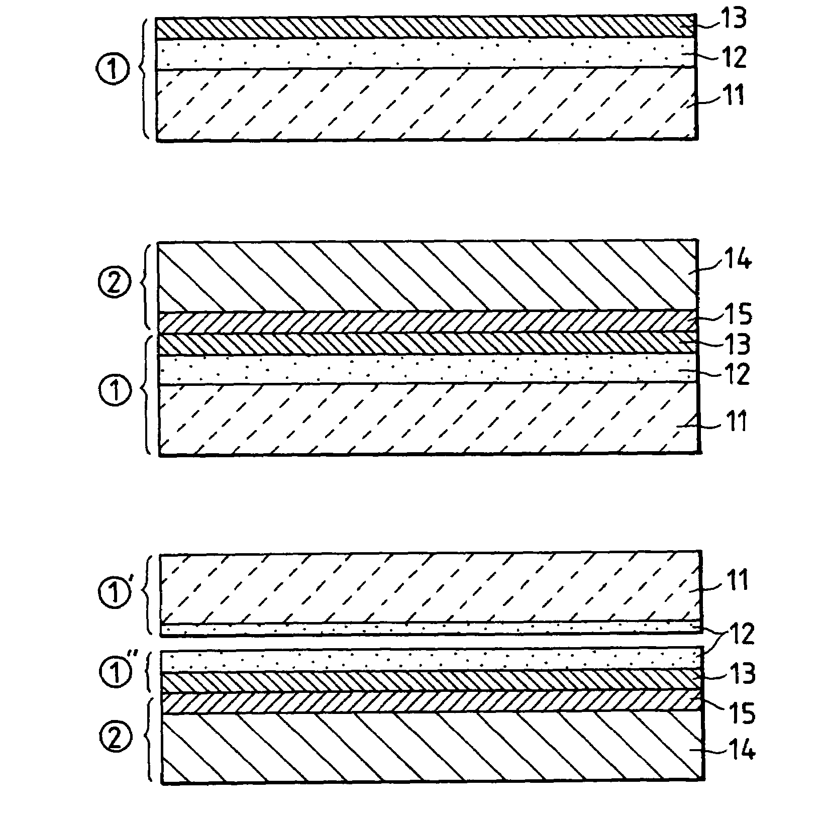
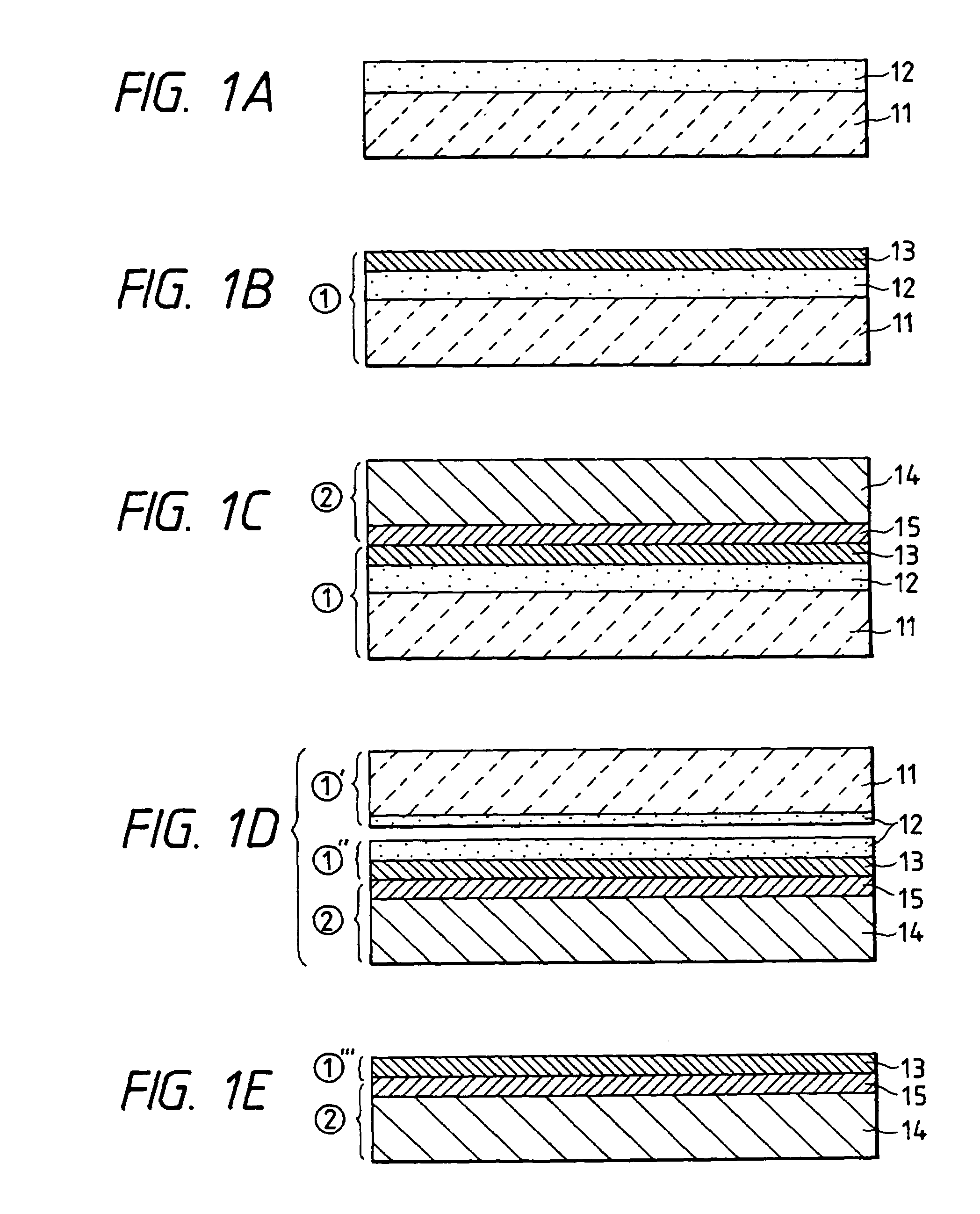
[0054]A first monocrystalline Si substrate 11 is made porous at the surface to form a porous layer 12 as shown in FIG. 1A. Then, nonporous monocrystalline Si layer 13 is formed on the porous Si layer 12 as shown in FIG. 1B.

[0055]Another Si supporting substrate 14 is brought into contact with the nonporous monocrystalline Si layer 13 with interposition of an insulative layer 15 at room temperature as shown in FIG. 1C, and then the contacted matter was subjected to anode coupling, compression, heat treatment, or combination thereof to bond tightly the Si supporting substrate 14 and the monocrystalline layer 13 with interposition of the insulative layer 15. The insulative layer 15 may be formed preliminarily on either one of the monocrystalline Si layer 13 or the Si supporting substrate 14, or the three sheets may be bonded with an insulative thin film interposed.

[0056]Subsequently, the substrates are separated at the porous Si layer 12 as shown in FIG. 1D. On the Si supporting substra...

embodiment 2

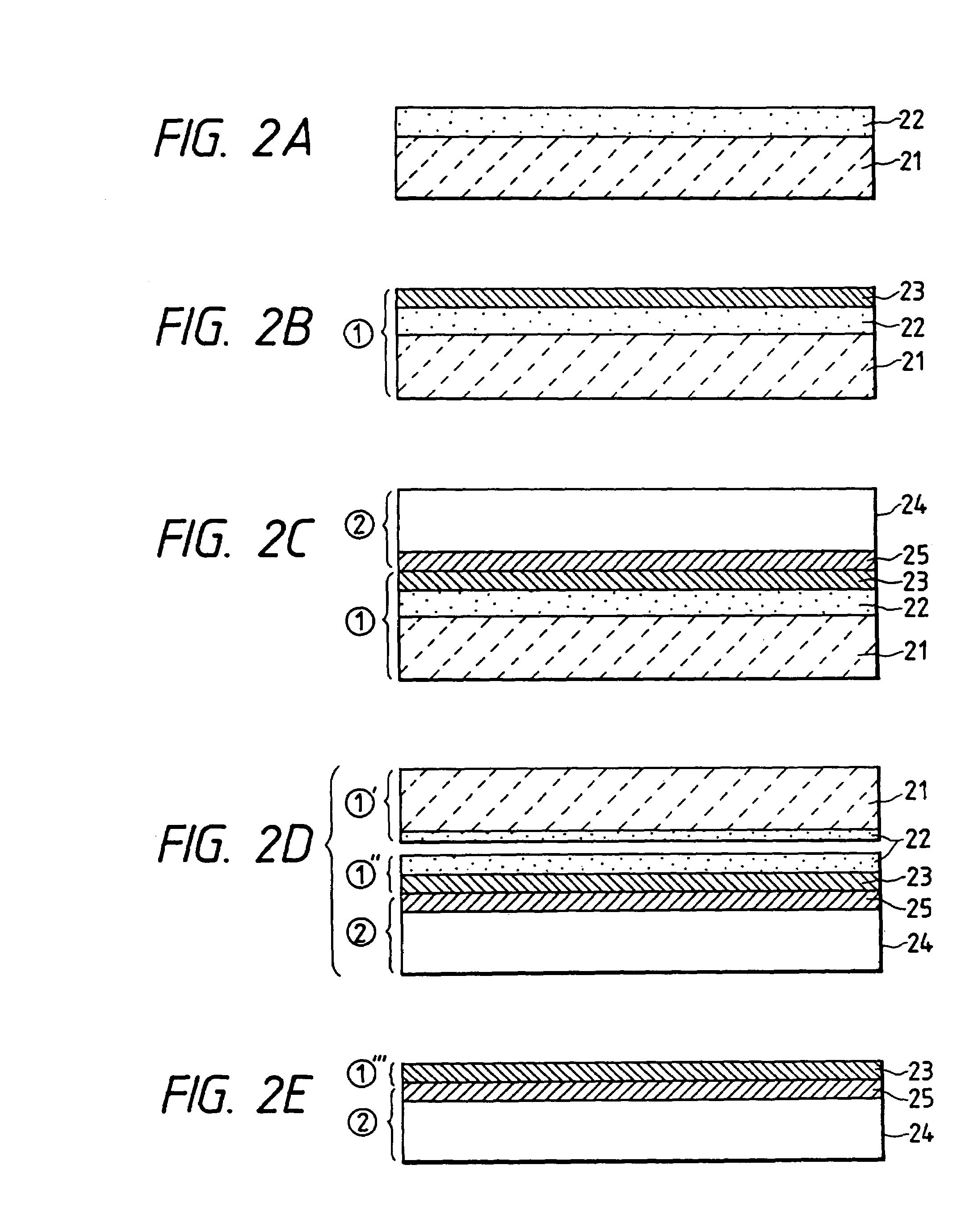
[0063]A first monocrystalline Si substrate 21 is made porous at the surface to form a porous layer 22 as shown in FIG. 2A. Then a nonporous monocrystalline Si layer 23 is formed on the porous Si layer 22 as shown in FIG. 2B.

[0064]A light-transmissive supporting substrate 24 is brought into contact with the monocrystalline Si layer 23 with interposition of an insulative layer 25 at room temperature as shown in FIG. 2C, and then the contacted matter was subjected to anode coupling, compression, heat treatment, or combination of the treatment to bond tightly the light-transmissive supporting substrate 24 and the monocrystalline layer 23 with interposition of the insulative layer 25. The insulative layer 25 may be formed preliminarily on either one of the monocrystalline Si layer or the light-transmissive supporting substrate 24, or the three sheets may be bonded with interposition of an insulative thin film.

[0065]Subsequently, the substrates are separated at the porous Si layer 22 as s...

embodiment 3

[0071]A first monocrystalline Si substrate 31 is made porous at the surface to form a porous layer 32 as shown in FIG. 3A. Then a nonporous monocrystalline compound semiconductor layer 33 is formed on the porous Si layer 32 as shown in FIG. 3B.

[0072]Another Si supporting substrate 34 is brought into close contact with the monocrystalline compound semiconductor layer 33 with interposition of an insulative layer 35 at room temperature as shown in FIG. 3C, and then the contacted matter was subjected to anode coupling, compression, or heat treatment, or combination of the treatments to bond tightly the Si supporting substrate 34 and the monocrystalline layer 33 with interposition of the insulative layer 35. The insulative layer 35 may be formed preliminarily on either one of the monocrystalline compound semiconductor layer or the Si supporting substrate 34, or the three sheets may be bonded with interposition of an insulative thin film.

[0073]Subsequently, the substrates are separated at...


PUM

PropertyMeasurementUnit
thicknessaaaaaaaaaa
porosityaaaaaaaaaa
densityaaaaaaaaaa

Abstract

A process for producing a semiconductor substrate is provided which comprises steps of forming a porous layer on a first substrate, forming a nonporous monocrystalline semiconductor layer on the porous layer of the first substrate, bonding the nonporous monocrystalline layer onto a second substrate, separating the bonded substrates at the porous layer, removing the porous layer on the second substrate, and removing the porous layer constituting the first substrate.

Description

[0001]This application is a division of application Ser. No. 08 / 863,717 filed May 27, 1997, U.S. Pat. No. 5,856,229, which is a continuation of application Ser. No. 08 / 401,237 filed Mar. 9, 1995, now abandoned.BACKGROUND OF THE INVENTION[0002]1. Field of the Invention[0003]The present invention relates to a process for producing a semiconductor substrate. More specifically, the present invention relates to a process for producing a monocrystalline semiconductor on a dielectric-isolated or insulative material, or a monocrystalline compound semiconductor on a semiconductor substrate. Further the present invention relates to a process for producing an electronic device or an integrated circuit formed on a single crystalline semiconductor layer.[0004]2. Related Background Art[0005]The technique of formation of monocrystalline Si (silicon) semiconductor on an insulative material is well known as silicon-on-insulator (SOI) technique. The device prepared by SOI technique has various advant...

Claims


Application Information

Patent Timeline
Patent Type & Authority Patents(United States)
IPC IPC(8): H01L23/12
CPCH01L21/6835H01L21/76259H01L2221/68363
Inventor SAKAGUCHI, KIYOFUMIYONEHARA, TAKAO
Owner CANON KK
Why Eureka
Try Eureka