Display apparatus, method of manufacturing the same, and method of driving the same

a technology of display apparatus and manufacturing method, applied in the field of display apparatus, can solve the problems of complex manufacturing process complexity and increase the cost of manufacturing process, and the inability to form desired liquid crystal domain, so as to prevent the response speed

Inactive Publication Date: 2012-09-06
SAMSUNG DISPLAY CO LTD
View PDF10 Cites 36 Cited by
  • Summary
  • Abstract
  • Description
  • Claims
  • Application Information

AI Technical Summary

Benefits of technology

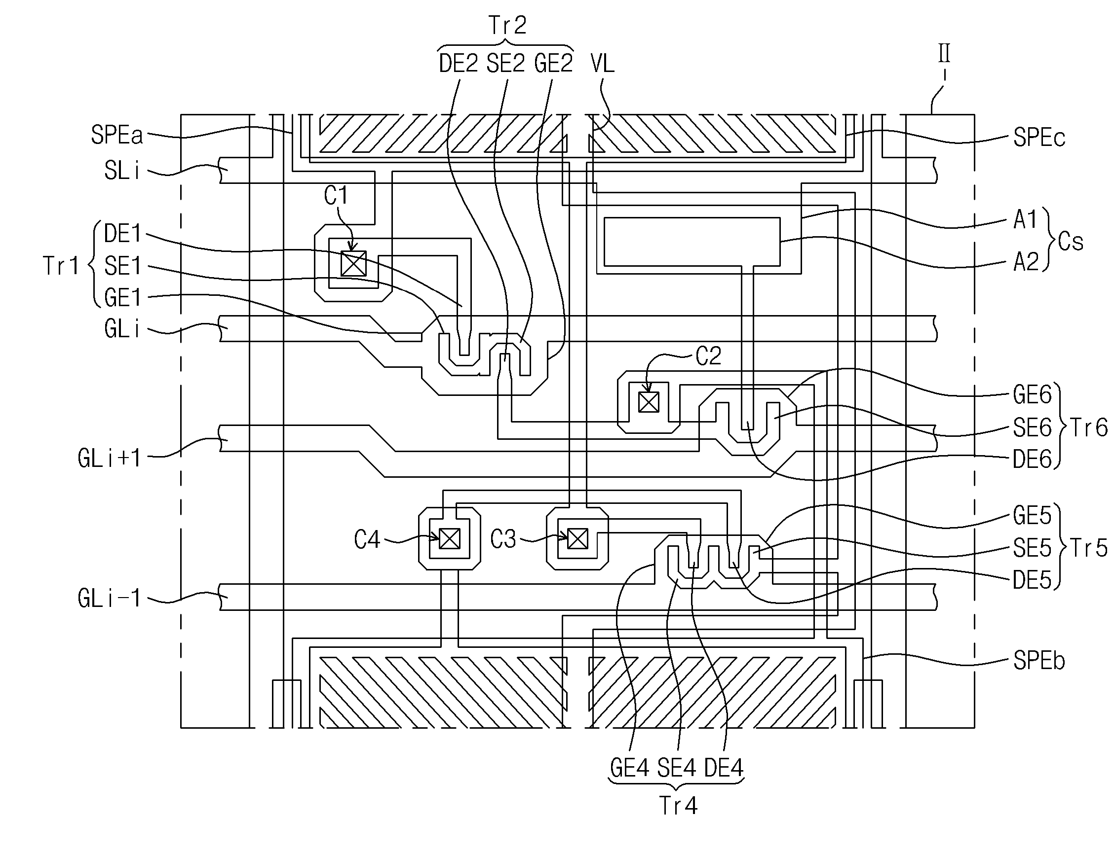
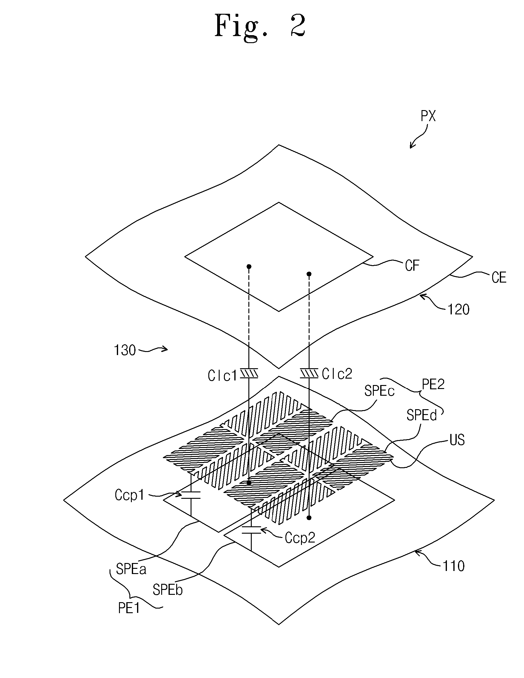
[0008]An exemplary embodiment provides a display apparatus capable of substantially or effectively preventing the formation of texture defects and improving response speed, and may have a structure in which a slit formed in a pixel electrode and a reference electrode is not patterned.
[0016]Thus, the display apparatus may substantially or effectively prevent the response speed from being delayed in the image display mode by the electric field and the formation of texture defects in the electric field exposure process.

Problems solved by technology

However, when the pixel electrode and the common electrode are patterned in order to form the liquid crystal domains, the complexity and cost of a manufacturing process is increased.
In addition, if a misalignment occurs between the pixel electrode and the common electrode, the desired liquid crystal domain is not formed.

Method used


Image

  • Display apparatus, method of manufacturing the same, and method of driving the same
  • Display apparatus, method of manufacturing the same, and method of driving the same
  • Display apparatus, method of manufacturing the same, and method of driving the same

Examples


Embodiment Construction

[0034]It will be understood that when an element or layer is referred to as being “on”, “connected to” or “coupled to” another element or layer, it can be directly on, connected or coupled to the other element or layer, or intervening elements or layers may be present. In contrast, when an element is referred to as being “directly on,”“directly connected to” or “directly coupled to” another element or layer, there are no intervening elements or layers present. Like numbers refer to like elements throughout. As used herein, the term “and / or” includes any and all combinations of one or more of the associated listed items.

[0035]It will be understood that, although the terms first, second, etc. may be used herein to describe various elements, components, regions, layers, and / or sections, these elements, components, regions, layers and / or sections should not be limited by these terms. These terms are only used to distinguish one element, component, region, layer, or section from another ...


PUM

PropertyMeasurementUnit
temperatureaaaaaaaaaa

Abstract

A display apparatus includes a first substrate including a first base substrate, a first pixel electrode disposed on the first base substrate, an insulating layer on the first pixel electrode, and a second pixel electrode disposed on the insulating layer and including a plurality of slits; a second substrate including a second base substrate opposite the first base substrate and on the first base substrate, and a reference electrode disposed on the second base substrate and facing the second pixel electrode; and a liquid crystal layer is disposed between the second pixel electrode and the reference electrode, the liquid crystal layer including liquid crystal molecules which are vertically aligned relative to the first and second substrates.

Description

CROSS-REFERENCE TO RELATED APPLICATION[0001]This application claims priority to Korean Patent Application No. 10-2011-0019555, filed on Mar. 4, 2011, and all the benefits accruing therefrom under 35 U.S.C. §119, the content of which in its entirety is herein incorporated by reference.BACKGROUND OF THE INVENTION[0002]1. Field of the Invention[0003]This disclosure relates to a display apparatus capable of preventing the formation of texture defects and improving response speed, a method of manufacturing the display apparatus, and a method of driving the display apparatus.[0004]2. Description of the Related Art[0005]In general, a liquid crystal display includes two transparent substrates and a liquid crystal layer disposed between the two substrates. The alignment of the liquid crystal layer selected to control light transmittance of the liquid crystal layer in each pixel, thereby displaying a desired image.[0006]A driving mode of the liquid crystal display is a vertical alignment mode...

Claims


Application Information

Patent Timeline
Patent Type & Authority Applications(United States)
IPC IPC(8): G02F1/1337H01L33/08G02F1/1333
CPCG02F1/133707G02F1/134309G02F2001/134381G02F1/1395G02F2001/134345G02F1/13624G02F1/134381G02F1/134345G02F1/133753G02F1/136286G02F1/1368
Inventor JUNG, KWANG-CHULLEE, HYEOKJINKWON, OHJEONG
Owner SAMSUNG DISPLAY CO LTD
Why Eureka
Try Eureka