Transflective liquid crystal display device

a liquid crystal display device and transflective technology, applied in non-linear optics, instruments, optics, etc., can solve the problems of inability to control, visible defect called “bright dot defect”, and the transflective liquid crystal display device of patent document 2 is susceptible to inter-surface short-circuiting, so as to prevent prevent the reduction of reflective contrast, and maintain the effect of reducing the formation of bright dot defects

Inactive Publication Date: 2008-01-01
MITSUBISHI ELECTRIC CORP
View PDF33 Cites 1 Cited by
  • Summary
  • Abstract
  • Description
  • Claims
  • Application Information

AI Technical Summary

Benefits of technology

[0019]An object of the present invention is to provide a transflective liquid crystal display device in which source bus lines and reflective pixel electrodes are formed in the same layer and separated at given intervals, and reflective contrast reduction preventing electrodes are formed in given positions in order to prevent reduction of reflective contrast, for example, and the transflective liquid crystal display device is capable of preventing formation of bright dot defects while maintaining the reflective contrast reduction prevention.
[0021]Even when the reflective contrast reduction preventing electrode is short-circuited with an opposing electrode formed on the second substrate, the opposing electrode is not electrically short-circuited with a transmissive electrode (that is, an inter-surface short-circuit is prevented). This prevents formation of very noticeable defects called bright dot defects. In other words, the transflective liquid crystal display device allows manufacture with high yield. The reflective contrast reduction preventing electrode forms a capacitance with the reflective electrode. Accordingly, a voltage can be applied to the reflective contrast reduction preventing electrode on the basis of the capacitance. This allows normal application of an electric field to the liquid crystal layer above the given spaces mentioned above, which prevents reduction of reflective contrast in the given spaces.

Problems solved by technology

Then, it is not possible to control, with an electric field, the light entering the display area and reflected at the storage capacitance electrode and the like existing under that interval.
The backlight coming out through the display area results in a very noticeable defect called “a bright dot defect”.
Therefore, the transflective liquid crystal display device of the Patent Document 2 is susceptible to inter-surface short-circuiting caused by contamination by foreign matter.
Accordingly, the transflective liquid crystal display device of Patent Document 2 is susceptible also to inter-surface short-circuiting caused by abnormalities of the color filter pattern (abnormalities of the color filter pattern cause deformation of the opposing electrode).
That is, the transflective liquid crystal display device of Patent Document 2 is prone to bright dot defects because of the positioning of the reflective contrast reduction preventing electrodes, which leads to reduction of yield and hence to increased manufacturing costs.

Method used


Image

  • Transflective liquid crystal display device
  • Transflective liquid crystal display device
  • Transflective liquid crystal display device

Examples


first preferred embodiment

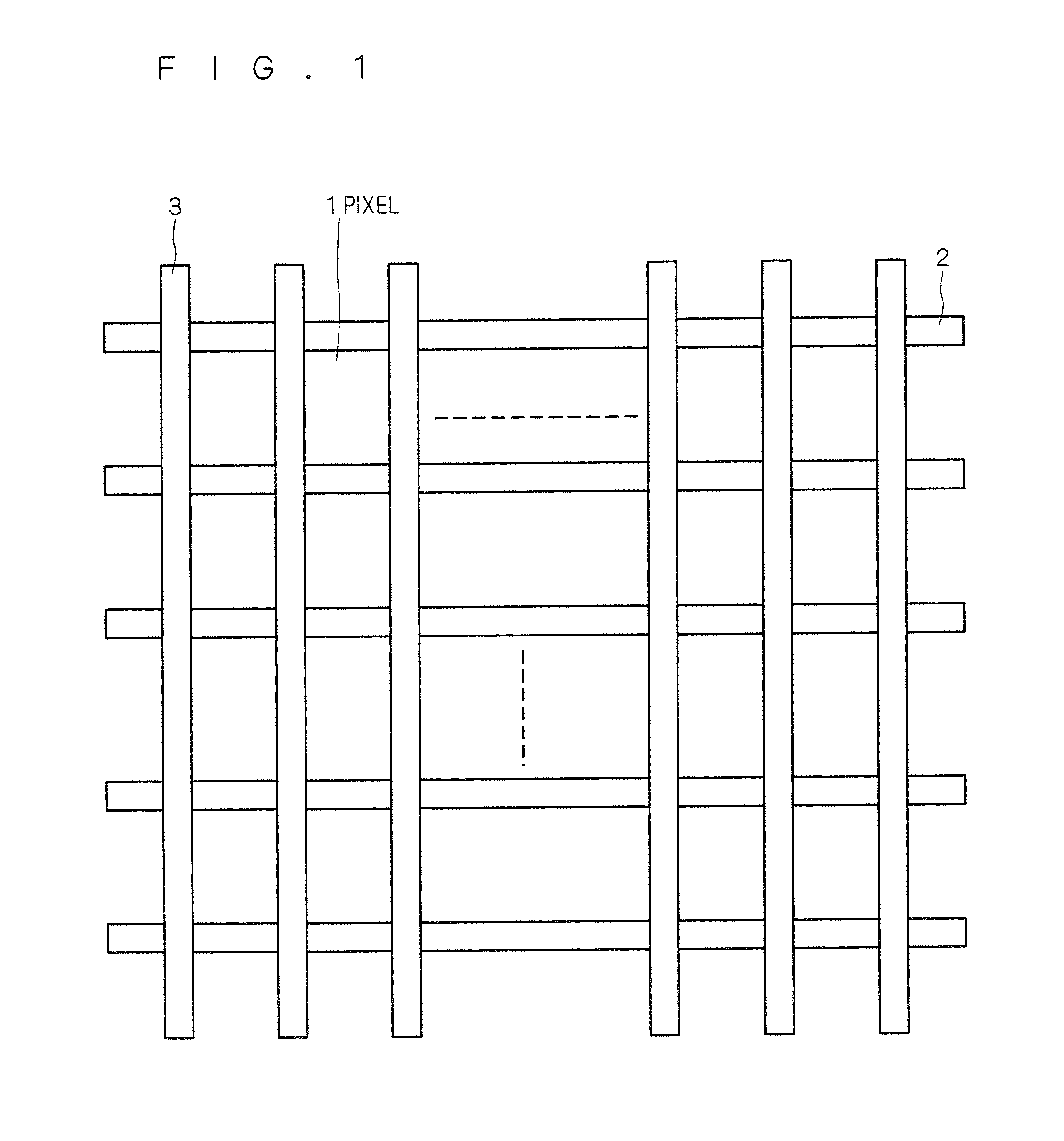
[0036]FIG. 1 is a plane view schematically illustrating the structure of a TFT (Thin Film Transistor) array substrate of a transflective liquid crystal display device according to a first preferred embodiment.

[0037]As shown in FIG. 1, a plurality of gate bus lines 2 are disposed in stripes on a transparent insulative substrate (not shown, which is regarded as a first substrate). Also on the transparent insulative substrate, a plurality of source bus lines 3 are disposed in stripes intersecting with the gate bus lines 2 in plane view.

[0038]The areas sectioned by the gate bus lines 2 and source bus lines 3 form pixel regions (i.e., unit pixels). As shown in FIG. 1, the unit pixel regions (hereinafter referred to simply as pixel regions) are disposed in a matrix.

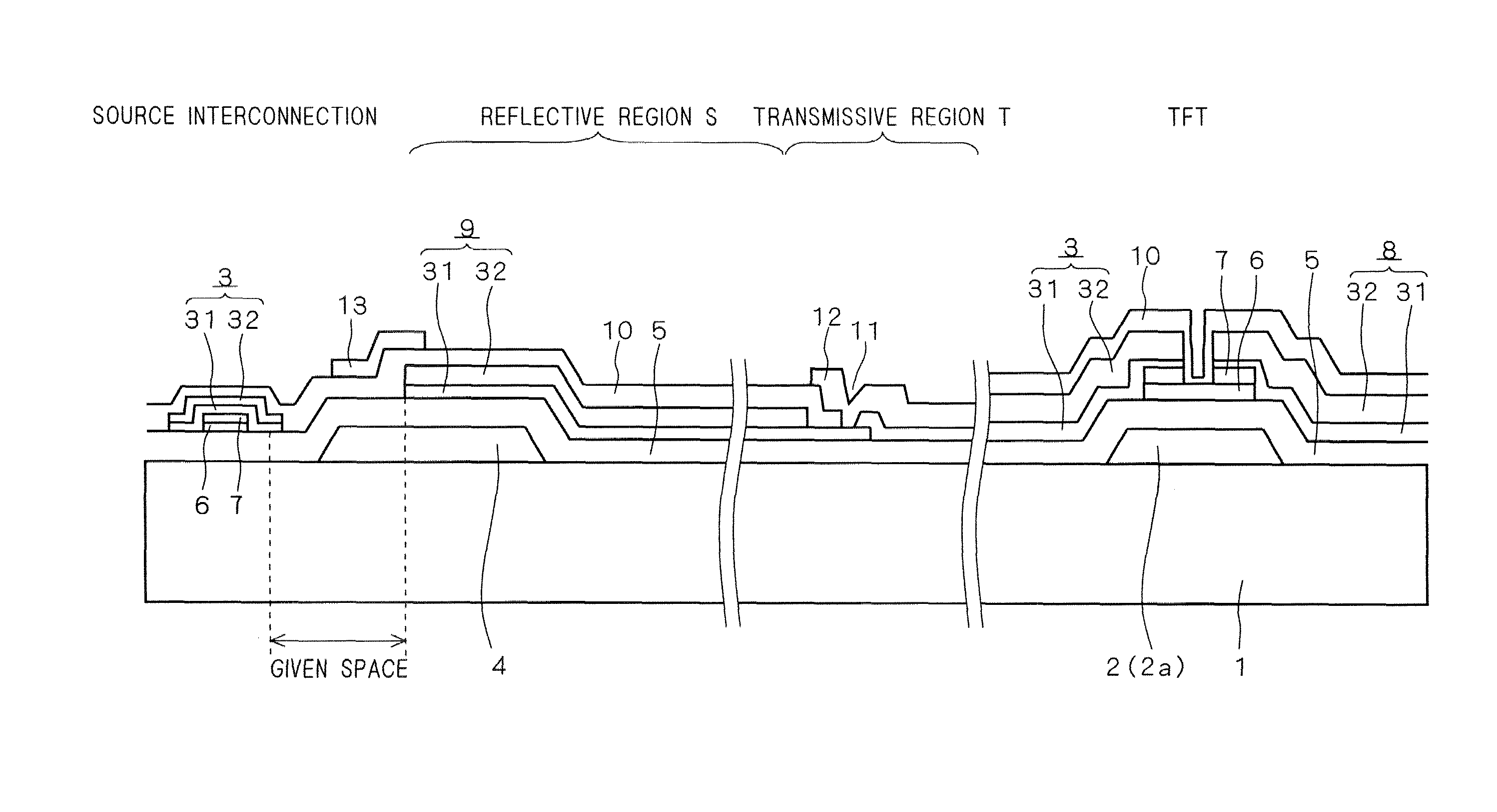
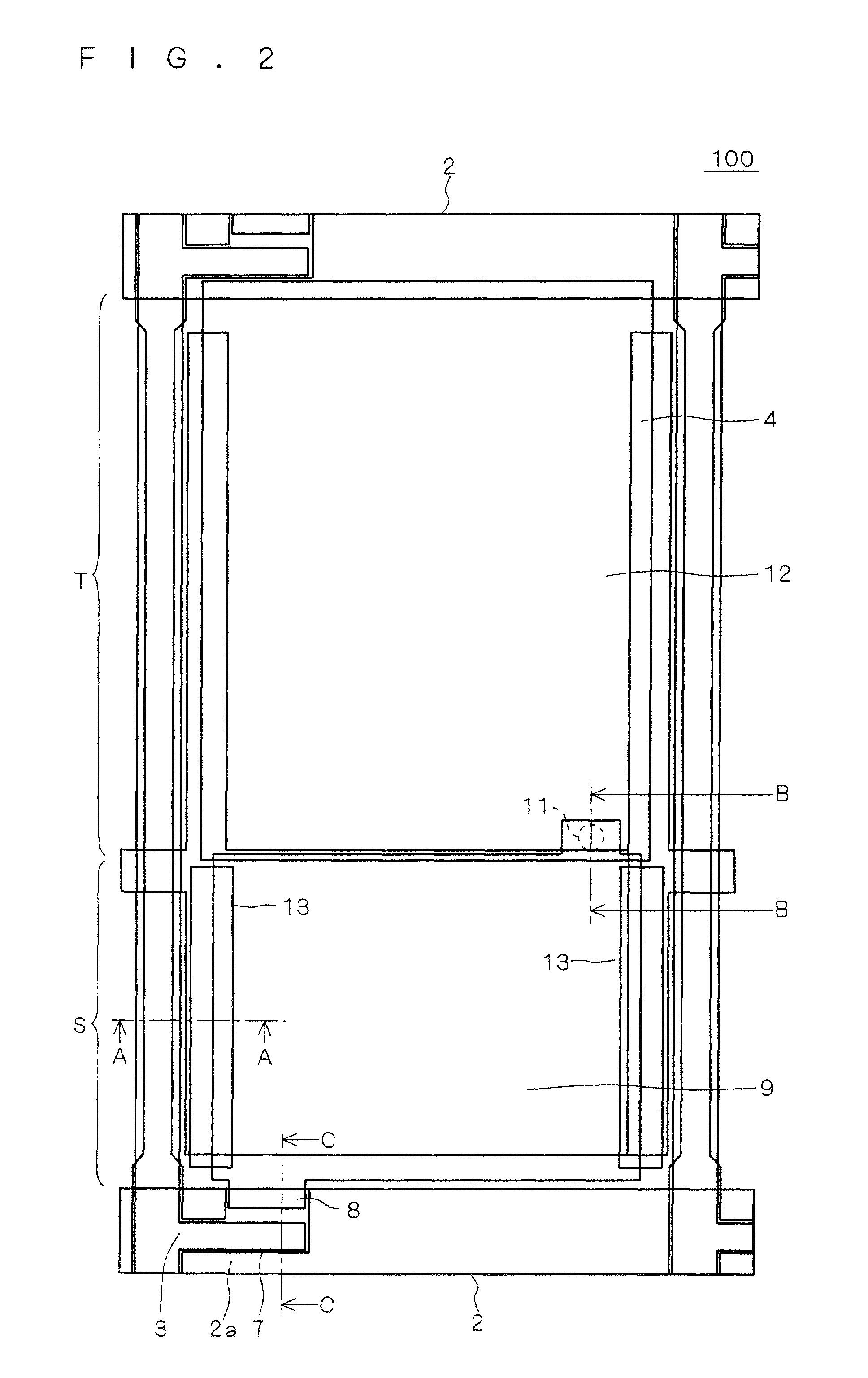
[0039]FIG. 2 is a plane view showing one pixel of the TFT array substrate of FIG. 1 in an enlarged manner. FIG. 3 shows sections of the TFT array substrate 100 of FIG. 2, including a section taken along line A-A (from a source ...

second preferred embodiment

[0126]As above, a given voltage is applied to the reflective contrast reduction preventing electrode 13 on the basis of the capacitance formed between the reflective contrast reduction preventing electrode 13 and the reflective electrode 9.

[0127]On the other hand, as mentioned earlier, the transflective liquid crystal display device of the first preferred embodiment has the storage capacitance electrodes 4 that function to hold voltage for a given period. As shown in FIG. 3 etc., the storage capacitance electrode 4 overlaps the reflective contrast reduction preventing electrode 13 in plane view, with the insulating films 5 and 10 existing between them. That is, a capacitance is formed also between the storage capacitance electrode 4 and the reflective contrast reduction preventing electrode 13.

[0128]Accordingly, the value of the voltage applied to the reflective contrast reduction preventing electrode 13 varies depending on the capacitance ratio between the electric capacitance C1 f...

third preferred embodiment

[0143]FIG. 11 is a plane view showing the structure of a transflective liquid crystal display device according to a third preferred embodiment. The TFT array substrate 150 of this preferred embodiment is structured almost the same as the TFT array substrate 100 of the first preferred embodiment. However, the TFT array substrate 150 differs from the TFT array substrate 100 in the following respect.

[0144]The description below shows only the difference, and other common components are not described here again. In this preferred embodiment, the components of the transflective liquid crystal display device other than the TFT array substrate 150 are the same as those of the first preferred embodiment.

[0145]As shown in FIG. 11, in the reflective region S of one pixel region, the TFT array substrate 150 of this preferred embodiment further includes a connection electrode 40. The connection electrode 40 is a member that electrically connects reflective contrast reduction preventing electrode...


PUM

PropertyMeasurementUnit
thicknessaaaaaaaaaa
thicknessaaaaaaaaaa
thicknessaaaaaaaaaa

Abstract

The present invention provides a transflective liquid crystal display device that has reflective contrast reduction preventing electrodes formed in given positions and that is capable of preventing bright dot defects while preventing reduction of reflective contrast. In a reflective region in a pixel region, a reflective electrode is formed in the same layer as source bus lines and separated by given spaces from the source bus lines. Reflective contrast reduction preventing electrodes are formed above the given spaces and have areas overlapping the reflective electrode in plane view, with an insulating film formed between them. The reflective contrast reduction preventing electrodes are in an electrically floating state.

Description

BACKGROUND OF THE INVENTION[0001]1. Field of the Invention[0002]The present invention relates to a transflective liquid crystal display device having a transmissive region transmitting backlight and a reflective region reflecting ambient light that are formed in pixel region.[0003]2. Description of the Background Art[0004]A transflective liquid crystal display device has a TFT (Thin Film Transistor) array substrate. On the array substrate, each pixel has a transmissive region that transmits backlight emitted from the rear side of the display surface and a reflective region that reflects ambient light coming into the liquid crystal layer.[0005]In a conventional technique for transflective liquid crystal display devices thus structured, reflective electrodes in the reflective regions, source bus lines (including source electrodes), and drain electrodes are formed in the same layer (see Japanese Patent Application No. 2004-110299, which is hereinafter referred to as Patent Document 1)....

Claims


Application Information

Patent Timeline
Patent Type & Authority Patents(United States)
IPC IPC(8): G02F1/1335
CPCG02F1/133553G02F1/136213G02F2203/09G02F1/1335
Inventor MASUTANI, YUICHINAGANO, SHINGO
Owner MITSUBISHI ELECTRIC CORP
Why Eureka
Try Eureka