Method for suppressing lattice defects in a semiconductor substrate

a technology of semiconductor substrate and lattice, applied in the field of semiconductor substrate fabrication, can solve problems such as crystal damage, and achieve the effect of suppressing the formation of leakage-promoting defects

Inactive Publication Date: 2010-02-04
SYNOPSYS INC
View PDF53 Cites 1 Cited by
  • Summary
  • Abstract
  • Description
  • Claims
  • Application Information

AI Technical Summary

Benefits of technology

[0004]An aspect of the claimed invention is a method for suppressing the formation of leakage-promoting defects in a crystal lattice following dopant implantation in the lattice. The process provides a compressive layer of atoms, these atoms having a size greater than that of the lattice member atoms. The lattice is then annealed for a time sufficient for interstitial defect atoms to be emitted from the compressive layer, and in that manner energetically stable defects are formed in the lattice at a distance from the compressive layer.

Problems solved by technology

It can be immediately gathered that such bombardment introduces crystal damage, in which lattice atoms are knocked out of lattice sites, while at the same time a certain number of the newly-introduced atoms will likewise come to rest in positions outside the lattice positions.

Method used


Image

  • Method for suppressing lattice defects in a semiconductor substrate
  • Method for suppressing lattice defects in a semiconductor substrate
  • Method for suppressing lattice defects in a semiconductor substrate

Examples


Embodiment Construction

[0011]The following detailed description is made with reference to the figures. Preferred embodiments are described to illustrate the present invention, not to limit its scope, which is defined by the claims. Those of ordinary skill in the art will recognize a variety of equivalent variations on the description that follows.

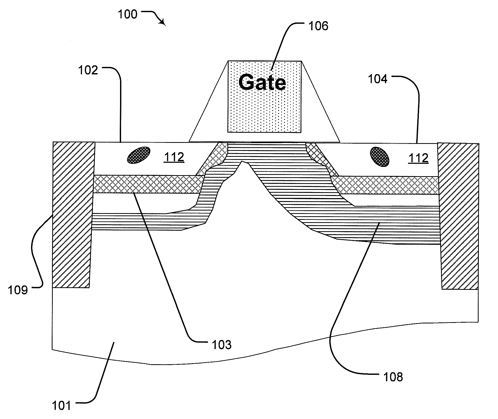
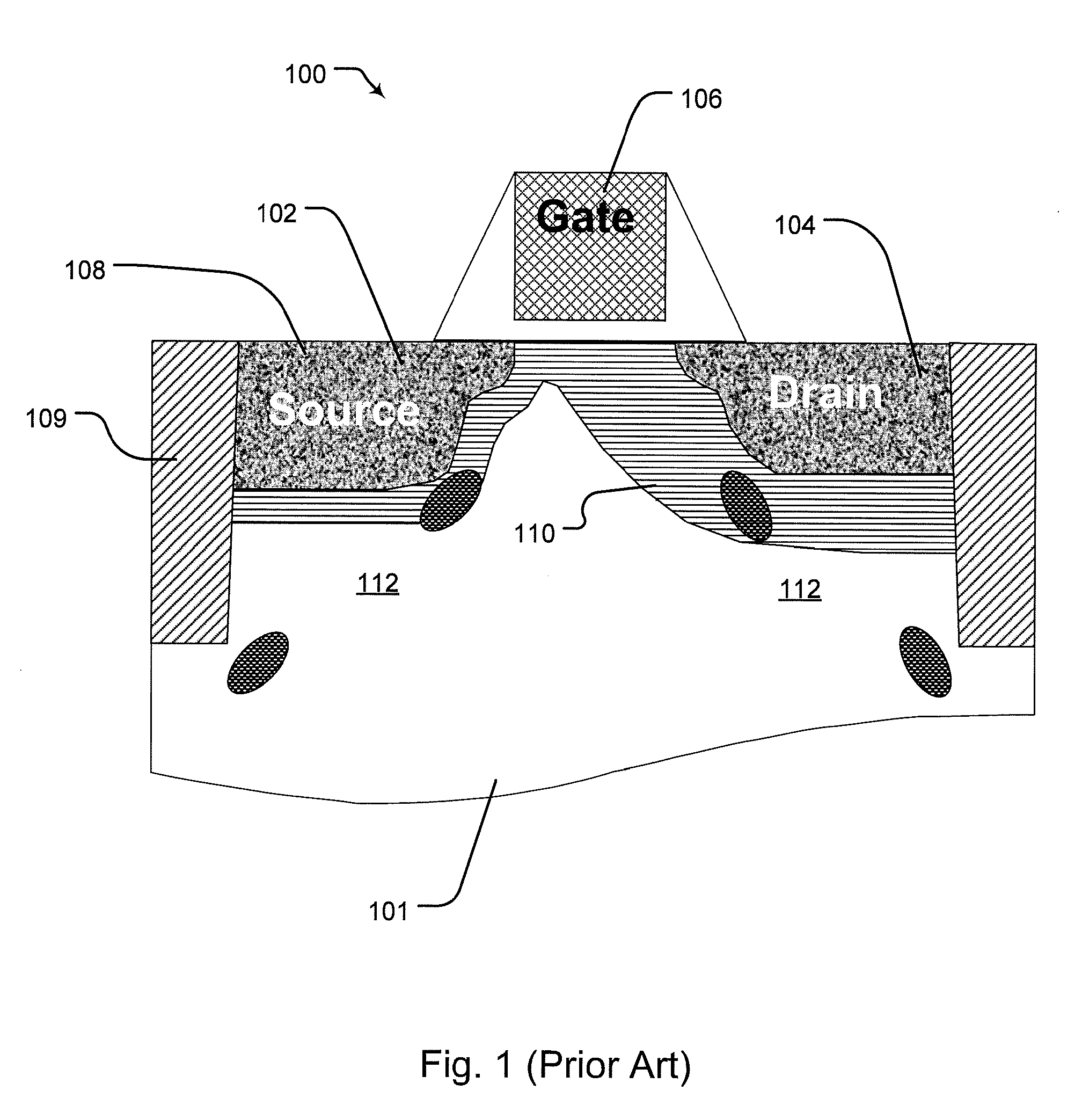
[0012]The problem addressed by the present disclosure is seen in FIG. 1, which depicts a typical MOSFET 100 after undergoing ion implantation. The transistor is formed on a silicon substrate 101 and includes source 102, drain 104 and gate 106. The depletion layer 108 adjacent each electrode and extending across the channel between the source and drain, is well known in the art. The depicted cell is one member of an array that can encompass millions of cells, as known in the art, and the cell is separated from other members of the array by Shallow Trench Isolators (STI) 109, filled with dielectric fill material.

[0013]The source and drain are formed in the silicon ...


PUM


Abstract

A method for suppressing the formation of leakage-promoting defects in a crystal lattice following dopant implantation in the lattice. The process provides a compressive layer of atoms, these atoms having a size greater than that of the lattice member atoms. The lattice is then annealed for a time sufficient for interstitial defect atoms to be emitted from the compressive layer, and in that manner energetically stable defects are formed in the lattice at a distance from the compressive layer.

Description

BACKGROUND OF THE INVENTION[0001]The present invention relates to the field of semiconductor fabrication. In particular, it relates to the fabrication of field effect transistors (FETs), involving the formation of semiconductor materials of selected conductivity, carried on by implantation of dopants.[0002]Fabrication of metal oxide semiconductor (MOS) FETs requires the formation of source and drain regions in a substrate of generally pure silicon (Si). The Si is provided in the form of a wafer, grown as a single crystal. Zones of the Si lattice are converted into regions of N or P conductivity by the addition of donor-type dopants, such as arsenic, for N regions, and acceptor-type dopants, such as boron, for P regions. These dopants are generally introduced by ion bombardment, in which ionized dopant atoms are energized and fired at the lattice, penetrating the crystal structure to a depth largely dependent on the bombardment energy and the ion mass.[0003]It can be immediately gath...

Claims


Application Information

Patent Timeline
Patent Type & Authority Applications(United States)
IPC IPC(8): H01L29/78
CPCH01L21/26506H01L21/26513H01L29/7848H01L29/1054H01L29/1079H01L21/324
Inventor MOROZ, VICTORPRAMANIK, DIPANKAR
Owner SYNOPSYS INC
Why Eureka
Try Eureka