Apparatus for inspecting light emitting diode and inspecting method using said apparatus

a technology for inspecting apparatus and light emitting diodes, which is applied in the direction of television systems, semiconductor/solid-state device testing/measurement, instruments, etc., can solve the problems of preventing high-speed inspection of emission characteristics, increasing the rate of led defects, and affecting the inspection efficiency of leds. the effect of inspection costs

Active Publication Date: 2012-10-04
SAMSUNG ELECTRONICS CO LTD
View PDF1 Cites 37 Cited by
  • Summary
  • Abstract
  • Description
  • Claims
  • Application Information

AI Technical Summary

Benefits of technology

[0008]An aspect of the present invention provides an inspection apparatus for reducing inspection costs and enabling high speed inspection, by determining defects of an LED regarding appearance and emission characteristics, simultaneously, and an inspection method using the same.

Problems solved by technology

Consequently, a rate of defects occurring in the LED is also increasing.
However, since the emission characteristics cannot be inspected by the vision inspection, a dedicated inspection for the emission characteristics is necessary.
However, use of the mechanical shutter operation may hinder high-speed inspection of the emission characteristics.
In addition, the lifespan of the apparatus may be reduced while the UV lamp increases initial expenses and maintenance expenses.

Method used


Image

  • Apparatus for inspecting light emitting diode and inspecting method using said apparatus
  • Apparatus for inspecting light emitting diode and inspecting method using said apparatus
  • Apparatus for inspecting light emitting diode and inspecting method using said apparatus

Examples


Embodiment Construction

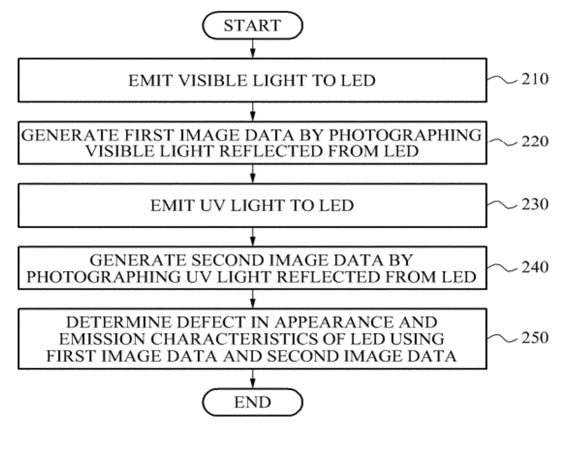
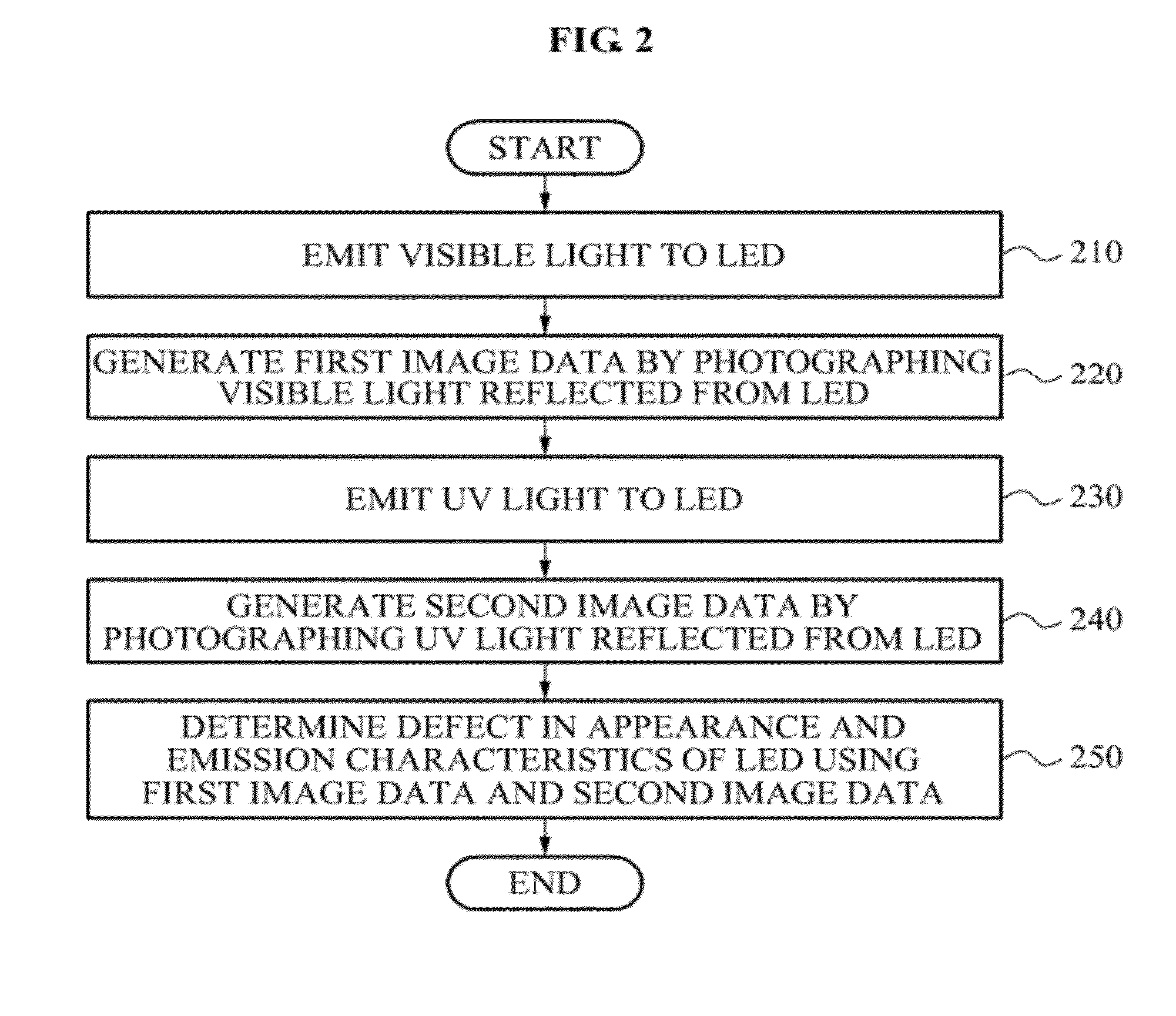
[0034]Reference will now be made in detail to exemplary embodiments of the present invention, examples of which are illustrated in the accompanying drawings, wherein like reference numerals refer to the like elements throughout. In the following description, when it is determined that a detailed description of well-known functions related to the present invention and the construction thereof would make the gist of the present invention obscure, they will be omitted. The terminology used herein is for the purpose of describing particular embodiments only and the definition may be varied according to the intention of a user, an operator, or customs. Therefore, the terms and words should be defined based on a description of this specification.

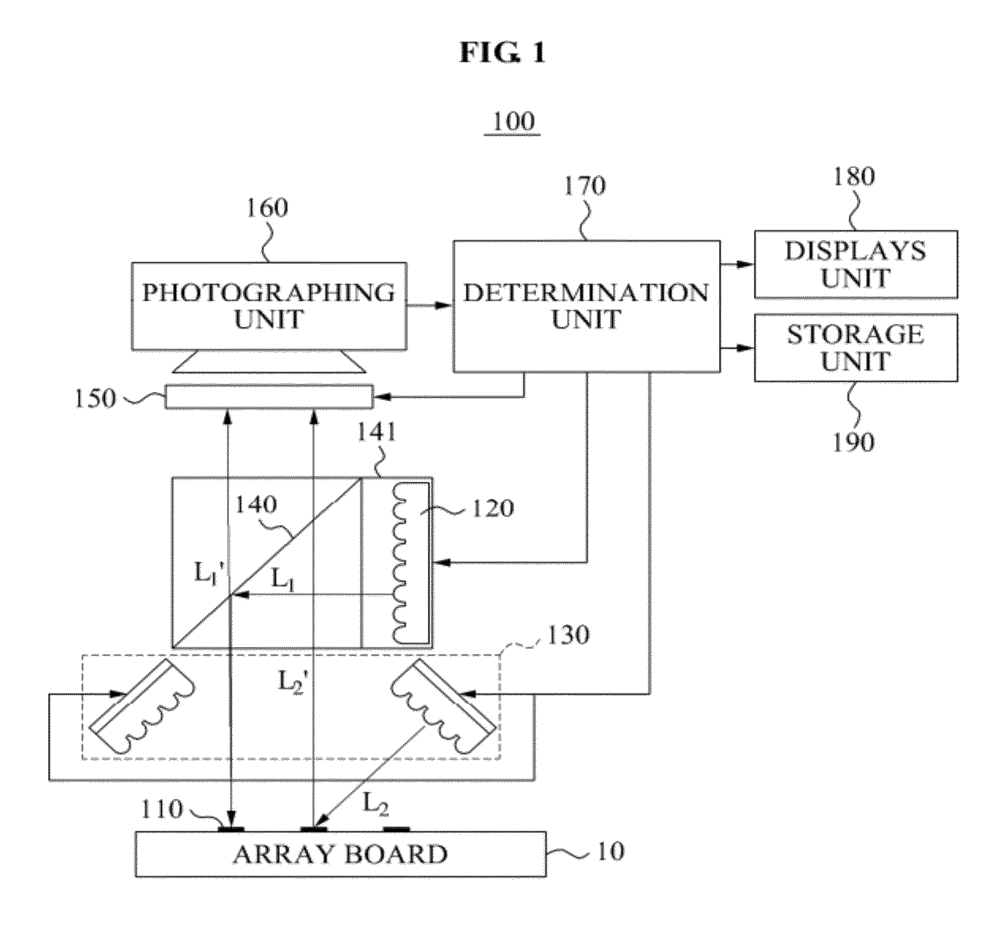
[0035]FIG. 1 is a block diagram illustrating a structure of a light emitting diode (LED) inspection apparatus according to an embodiment of the present invention. Referring to FIG. 1, the LED inspection apparatus 100 may include an LED 110, a firs...


PUM


Abstract

A light emitting diode (LED) inspection apparatus includes at least one LED including a phosphor applied on an emission surface, a first lighting unit to emit visible light to the LED, a second lighting unit to emit ultraviolet (UV) light to the LED, a photographing unit to generate at least one first image data by photographing the visible light reflected from the LED and to generate at least one second image data by photographing the UV light reflected from the LED, and a determination unit to determine a defect in appearance and emission characteristics of the LED using the at least one first image data and second image data.

Description

CROSS-REFERENCE TO RELATED APPLICATION[0001]This application claims the benefit of Korean Patent Application No. 10-2011-0027761, filed on Mar. 28, 2011, in the Korean Intellectual Property Office, the disclosure of which is incorporated herein by reference.BACKGROUND[0002]1. Field of the Invention[0003]The present invention relates to an inspection apparatus for a light emitting diode (LED) and an inspection method using the same, and more particularly, to an inspection apparatus for determining inferiority of an LED by inspecting appearance and emission characteristics of the LED and an inspection method using the same.[0004]2. Description of the Related Art[0005]At first, a light emitting diode (LED) package had primarily been used for signaling. Recently, the LED package is applied more widely, for example, to lighting devices and a light source of a backlight unit (BLU) of a mobile phone or of a large-area display device such as a liquid crystal display (LCD). A demand for the ...

Claims


Application Information

Patent Timeline
Patent Type & Authority Applications(United States)
IPC IPC(8): H04N7/18
CPCG01N2021/8845G01N21/8806G01N21/956G01M11/0207G01R31/2635H01L22/00
Inventor JI, WON SOOKWON, OH SEOKKIM, CHOO HO
Owner SAMSUNG ELECTRONICS CO LTD
Why Eureka
Try Eureka