Packaging for fingerprint sensors and methods of manufacture

a fingerprint sensor and fingerprint technology, applied in the field of fingerprint sensor packaging and methods of manufacture, can solve the problem of difficult packaging of integrated circuits

Active Publication Date: 2012-10-11
AMKOR TECH SINGAPORE HLDG PTE LTD
View PDF6 Cites 90 Cited by
  • Summary
  • Abstract
  • Description
  • Claims
  • Application Information

AI Technical Summary

Problems solved by technology

Due to the exposed top surface, packaging of the integrated circuit can be difficult.

Method used


Image

  • Packaging for fingerprint sensors and methods of manufacture
  • Packaging for fingerprint sensors and methods of manufacture
  • Packaging for fingerprint sensors and methods of manufacture

Examples


Embodiment Construction

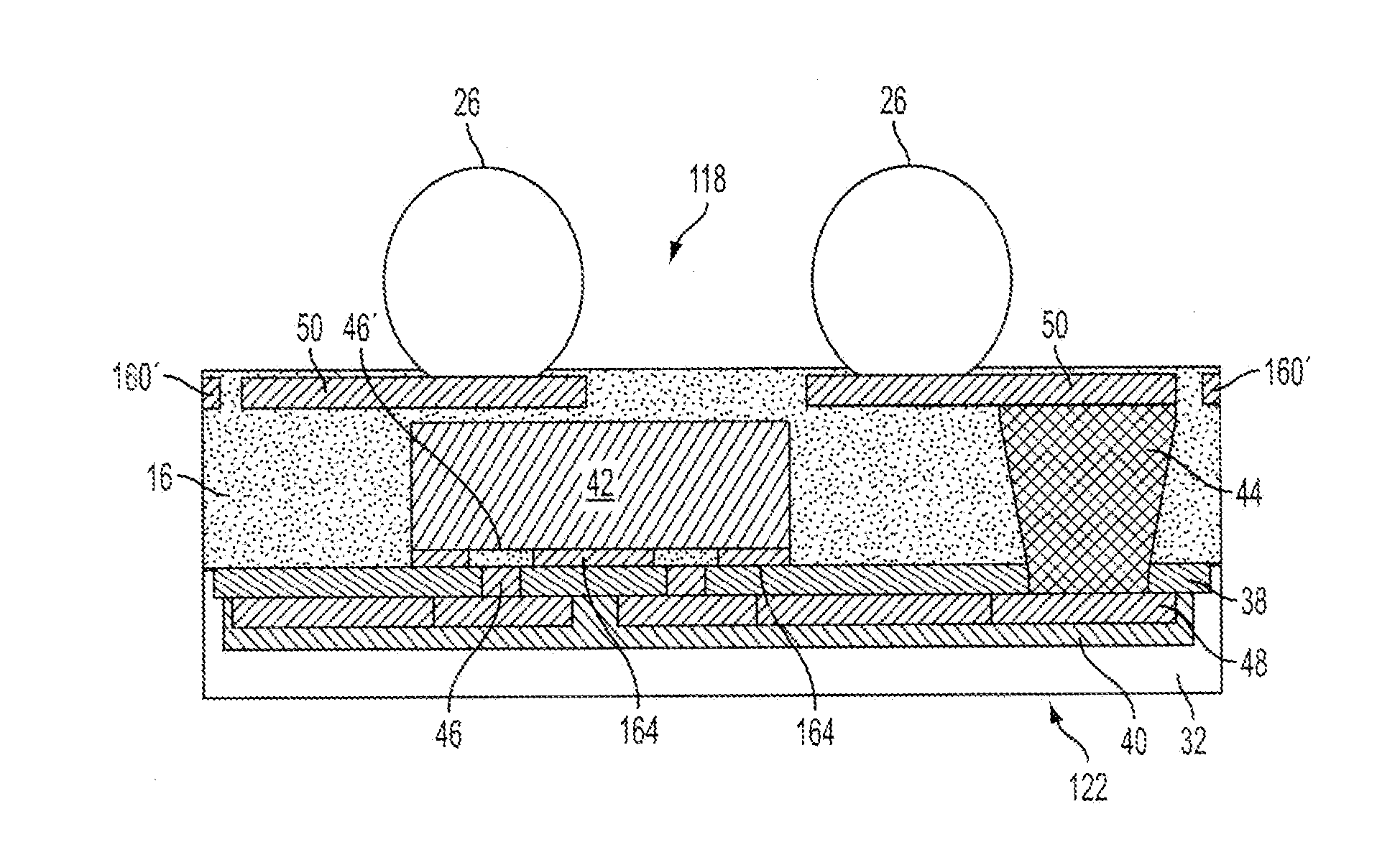
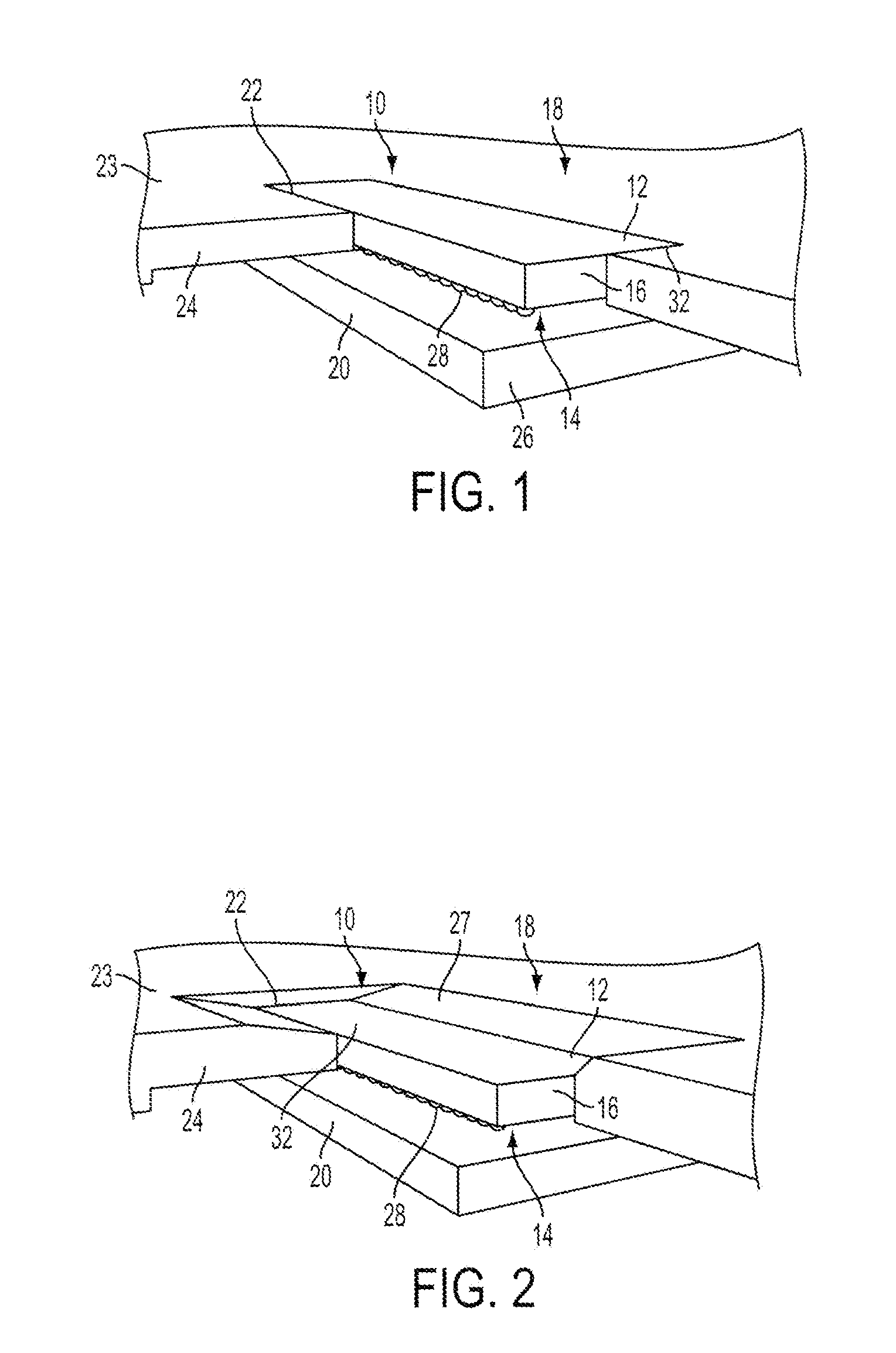
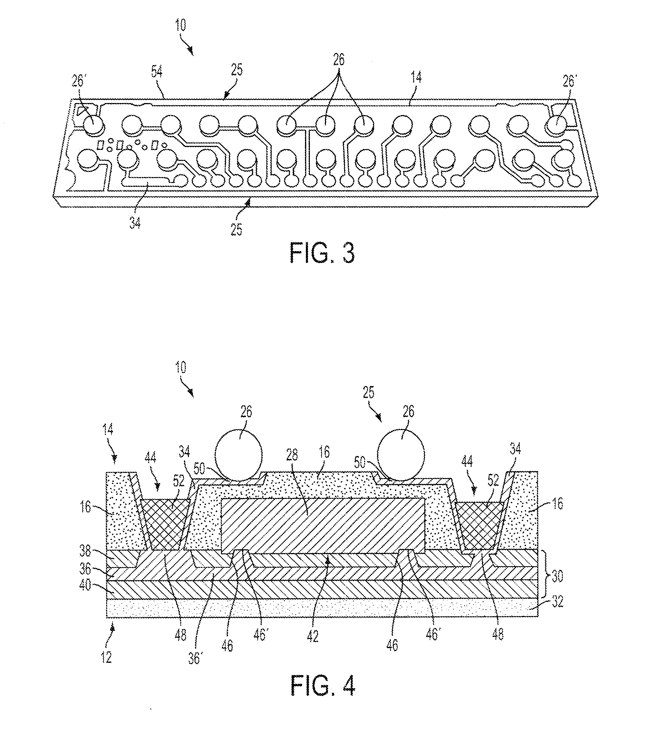
[0041]The following discussion is presented to enable a person skilled in the art to make and use embodiments of the disclosed subject matter. Various modifications to the illustrated embodiments will be readily apparent to those skilled in the art, and the generic principles herein can be applied to other embodiments and applications without departing from embodiments of the disclosed subject matter. Thus, embodiments of the disclosed subject matter are not intended to be limited to embodiments shown, but are to be accorded the widest scope consistent with the principles and features disclosed herein. The following detailed description is to be read with reference to the figures, in which like elements in different figures have like reference numerals. The figures, which are not necessarily to scale, depict selected embodiments and are not intended to limit the scope of embodiments of the disclosed subject matter. Skilled artisans will recognize the examples provided herein have ma...


PUM


Abstract

A fingerprint sensor package, including a sensing side for sensing fingerprint information and a separate connection side for electrically connecting the fingerprint sensor package to a host device, is disclosed. The fingerprint sensor package can also include a sensor integrated circuit facing the sensing side and substantially surrounded by a fill material. The fill material includes vias at peripheral locations around the sensor integrated circuit. The fingerprint sensor package can further include a redistribution layer on the sensing side which redistributes connections of the sensor integrated circuit to the vias. The connections can further be directed through the vias to a ball grid array on the connection side. Some aspects also include electrostatic discharge traces positioned at least partially around a perimeter of the connection side. Methods of manufacturing arc also disclosed.

Description

RELATED CASES[0001]This Application claims priority to U.S. Provisional Application 61 / 453,460, entitled PACKAGING FOR FINGERPRINT SENSORS AND METHODS OF MANUFACTURE, filed on Mar. 16, 2011, the disclosure of which is hereby incorporated by reference in its entirety for all purposes, as if the entire disclosure, specification and drawings, were completely reproduced in this application.BACKGROUND OF THE DISCLOSED SUBJECT MATTER[0002]Conventional fingerprint sensors include an integrated circuit, such as a silicon die, with an exposed top surface portion for receiving human touch. Due to the exposed top surface, packaging of the integrated circuit can be difficult. For example, conventional packages encapsulate the integrated circuit while exposing a portion of the top surface, but must provide room for wire connections from the top surface to peripheral connection points on a substrate below the integrated circuit. The substrate is provided with additional connection points in order...

Claims


Application Information

Patent Timeline
Patent Type & Authority Applications(United States)
IPC IPC(8): H01L23/485H01L21/768G06V30/144
CPCH01L21/561H01L21/568H01L23/3128G06K9/0002H01L24/19H01L2924/10253H01L2924/12041H01L24/96G06K9/00053H01L2924/00H01L2924/12042H01L2224/73267G06V40/1329G06V40/1306H01L21/56H01L23/28H01L23/31H01L23/481H01L23/60H01L24/97H01L24/17
Inventor ERHART, RICHARD ALEXANDERNELSON, RICHARD BRIAN
Owner AMKOR TECH SINGAPORE HLDG PTE LTD
Why Eureka
Try Eureka