
Light to current converter devices and methods of manufacturing the same

Active Publication Date: 2012-11-29
CSI CELLS CO LTD
View PDF5 Cites 17 Cited by
  • Summary
  • Abstract
  • Description
  • Claims
  • Application Information

AI Technical Summary

Benefits of technology

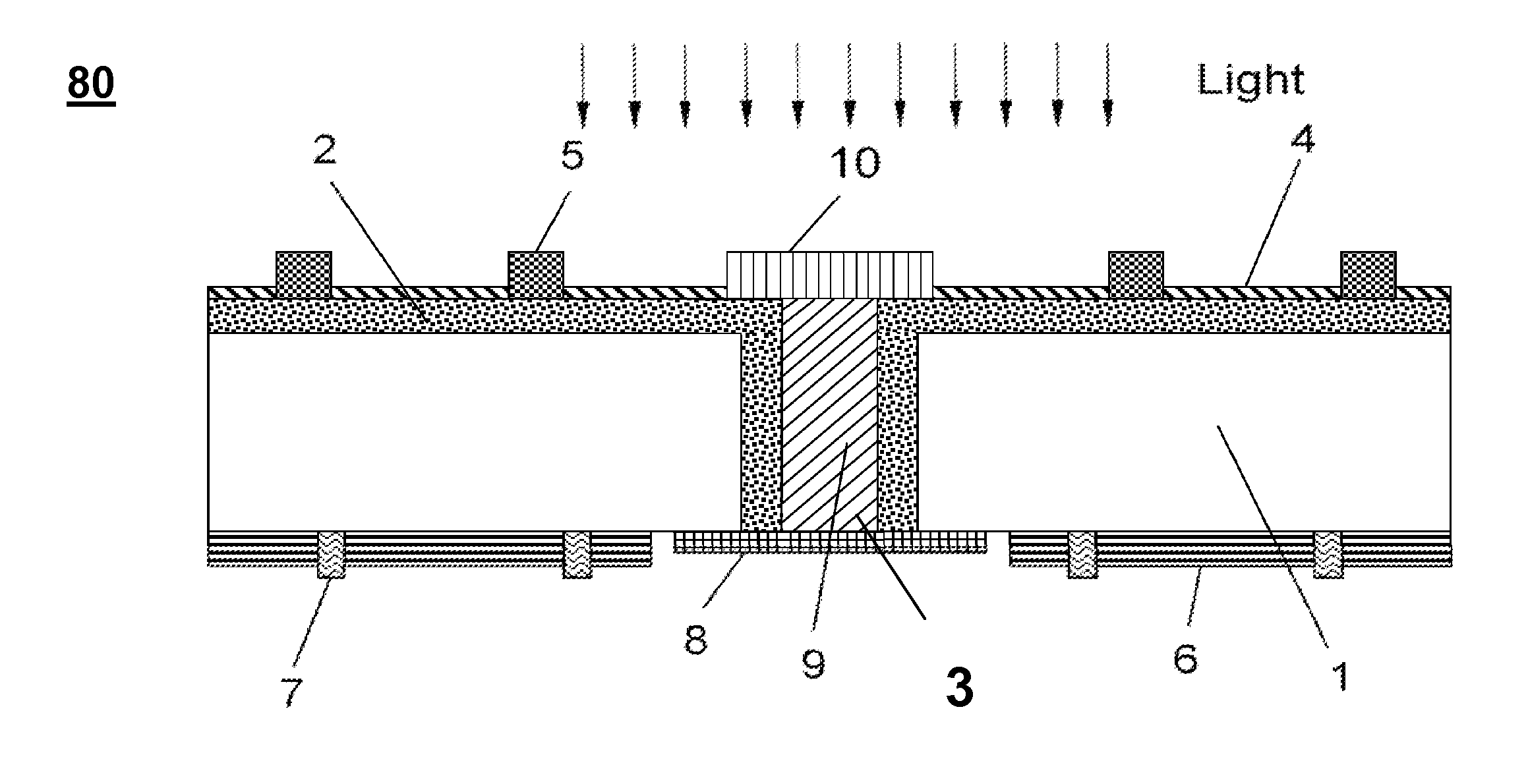
[0018]In some embodiments, the front surface of the semiconductor substrate may include a light-trapping structure for better light absorption. In some embodiments, the rear surface may further include an impurity layer of the first conductive type, wherein the impurity layer is insulated from the via rear collector.
[0027]In some embodiments, the front surface of the semiconductor substrate may include a light-trapping structure for better light absorption. In some embodiments, the rear surface may further include an impurity layer of the first conductive type, wherein the impurity layer may be insulated from the via rear collector.

Problems solved by technology

In recent years, interest in new forms of renewable energy has increased due to problems associated with conventional energy sources.
Therefore, shadow loss on the front or illuminated surface by the corresponding contacts limits the light to current conversion efficiency.
To generate this type of P-N junction, double sided diffusion is needed, causing throughput loss during manufacturing.
The use of the laser increases the breakage ratio of the solar cell, increases the production costs, and causes damage in the crystalline material leading to more recombination of charge carriers in the area around the laser groove.

Method used


Image

  • Light to current converter devices and methods of manufacturing the same
  • Light to current converter devices and methods of manufacturing the same
  • Light to current converter devices and methods of manufacturing the same

Examples


Embodiment Construction

[0060]The following description is presented to enable a person of ordinary skill in the art to make and use the various embodiments. Descriptions of specific devices, techniques, and applications are provided only as examples. Various modifications to the examples described herein will be readily apparent to those of ordinary skill in the art, and the general principles defined herein may be applied to other examples and applications without departing from the spirit and scope of the various embodiments. Thus, the various embodiments are not intended to be limited to the examples described herein and shown, but are to be accorded the scope consistent with the claims.

[0061]As used herein and in the appended claims, the singular forms “a,”“an,” and “the” include plural reference unless the context clearly indicates otherwise. Additionally, the terms “comprises” and “comprising” should be interpreted as referring to elements, components, or steps in a non-exclusive manner, indicating ...


PUM


Abstract

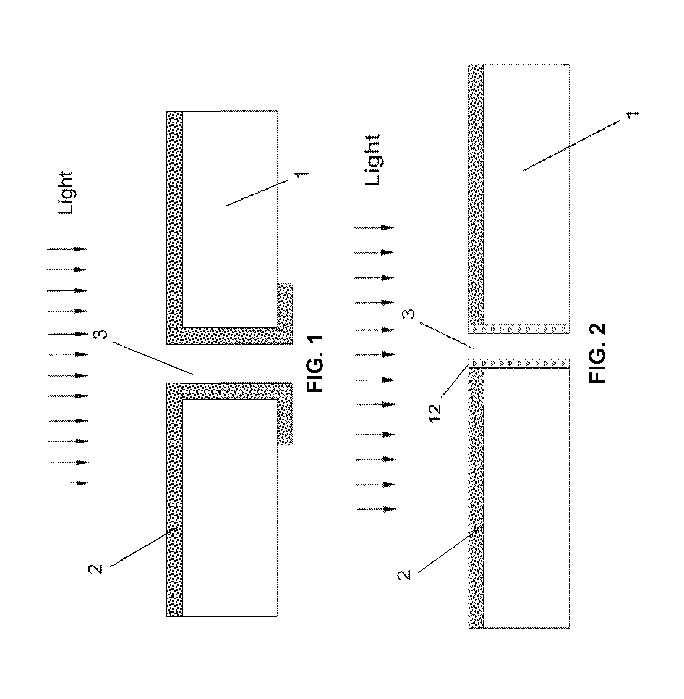
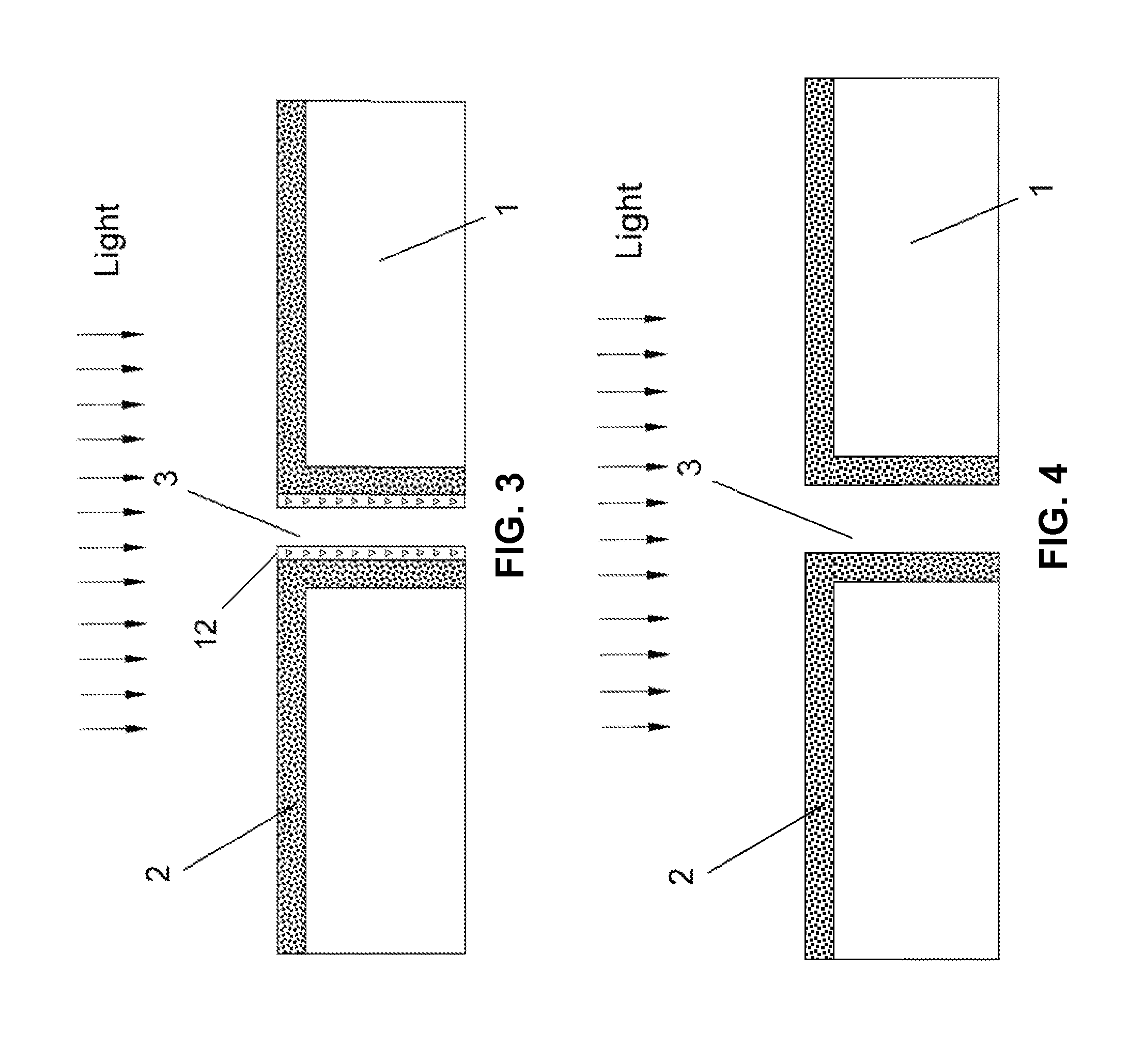
Light to current converter devices, such as solar cells, are disclosed. The devices may include via holes extending through the cell substrate and may include through-hole electrodes within the via holes. The through-hole electrodes may be made from one or more materials and may be hollow, partially hollow, or fully filled. Front and rear electrodes may also be formed on the device and can be made of the same or different materials as the through-hole electrode. The devices may include emitters located only on the top surface of the cell, located on the top surface and symmetrically or asymmetrically along a portion of the inner surface of the via holes, or located on the top surface and full inner surface of the via holes. Processes for making light to current converter devices are also disclosed.

Description

CROSS-REFERENCE TO RELATED APPLICATIONS[0001]This application claims the benefit of priority to Chinese Patent Application Numbers 201120175836.7, 201120176094.X, 201110141250.3, 201110141621.8, 201110141259.4, 201110141575.1, and 201110141248.6, filed May 27, 2011, which are incorporated by reference herein in their entirety. This application is also related to U.S. patent application Ser. No. ______ entitled “Methods of Manufacturing Light to Current Converter Devices” (Attorney Docket No. 69926-2000200), which is incorporated by reference herein in its entirety.BACKGROUND[0002]1. Field[0003]The present disclosure relates generally to light to current converter devices (e.g., solar cells), and, more particularly, to back contact solar cells.[0004]2. Related Art[0005]In recent years, interest in new forms of renewable energy has increased due to problems associated with conventional energy sources. For example, rising oil prices, global warming, exhaustion of fossil fuel energy, nu...

Claims


Application Information

Patent Timeline
IPC IPC(8): H01L31/0216H01L31/04H01L31/0236H01L31/0224
CPCH01L31/02245H01L31/1804H01L31/18Y02E10/547H01L31/022441Y02E10/542Y02P70/50
Inventor ZHANG, LINGJUNWU, JIANZHANG, FENGWANG, XUSHENG
Owner CSI CELLS CO LTD
Learn More