Manufacturing method of sulfur-silicon semiconductor alloy tandem solar cell

A technology of solar cells and semiconductors, applied in semiconductor/solid-state device manufacturing, semiconductor devices, circuits, etc., can solve problems such as high sheet resistance, large limitations, and long growth cycle, so as to improve processing efficiency and prevent external expansion and overflow , the effect of long growth cycle

Active Publication Date: 2018-02-06
SOUTHWEAT UNIV OF SCI & TECH +1
View PDF3 Cites 0 Cited by
  • Summary
  • Abstract
  • Description
  • Claims
  • Application Information

AI Technical Summary

Problems solved by technology

However, the heavy sulfur doping technology using femtosecond laser pulsed point light source in sulfur atmosphere is characterized by the formation of microstructure and heavy sulfur doping at the same time. The microstructure and sulfur doping interact with each other, and it is difficult to optimize the performance at the same time, resulting in black Silicon materials exhibit high light absorption and low photoelectric conversion efficiency
When the femtosecond laser interacts with silicon-based materials, the surface of the microstructure formed by multiple physical processes of liquefaction, vaporization, and deposition presents an amorphous structure, resulting in a sheet resistance as high as several thousand square ohms, which seriously affects the transport of carriers. The photovoltaic device formed has a large series resistance; and is heavily doped (concentration≧10 19 cm 3 ) The depth is limited, only 0.2-0.5µm, which affects infrared absorption, resulting in low photoelectric conversion efficiency, making the device performance far from being practical
[0004] Most patents at home and abroad are used to generate sulfur-doped silicon semiconductor amorphous silicon thin film layer by using femtosecond or picosecond pulsed laser spot. The inherent characteristics of the spot are in SF6 atmosphere, sulfur atoms are doped into the surface layer of the microstructure. During this physical conversion process, the silicon material will be violently vaporized, and the doped amount of sulfur element is low and unstable. It is very difficult to dope S atom concentration to 5×10¹⁸-1020 / cm3 in the amorphous layer with a thickness of micron scale. Big limitations
Long growth cycle and low efficiency

Method used


Image

  • Manufacturing method of sulfur-silicon semiconductor alloy tandem solar cell
  • Manufacturing method of sulfur-silicon semiconductor alloy tandem solar cell

Examples


Embodiment 1

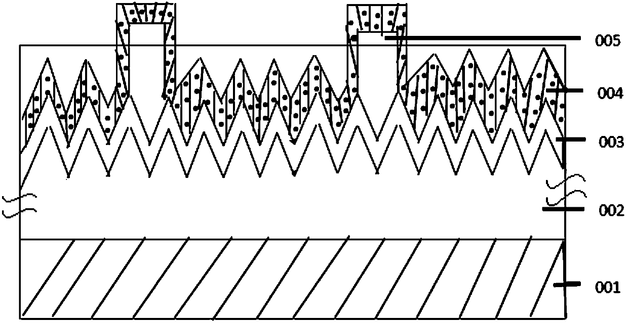
[0048] The present invention generates the structure of the submicron structure sulfur-silicon alloy laminated solar cell chip as follows figure 1 Shown:

[0049] 1. Al back field electrode,

[0050] 2. P-type Si layer,

[0051] 3. n-type Si layer,

[0052] 4. Sulfur-silicon semiconductor alloy layer (thickness 0.6µm),

[0053] 5. Collecting grid for commercial solar cell chips.

[0054] 1, 2, 3 and 5 are chip layers of commercial silicon-based solar cells.

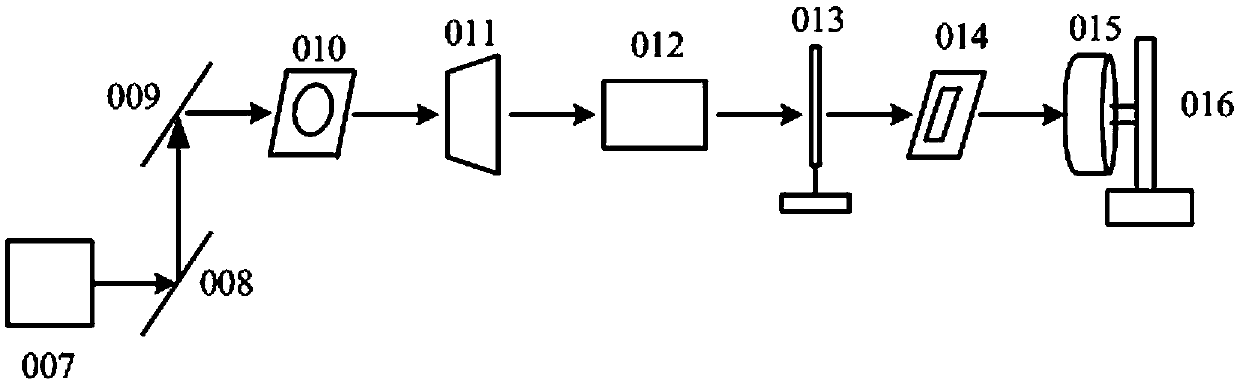
[0055] The structure of the laser band generating device of the present invention is as follows figure 2 Shown:

[0056] The laser band generation device sends laser light from the nanosecond laser 7 through the first and second 45-degree total reflection mirrors 8 and 9, the small hole 10, the beam expander 11, the attenuation sheet 12, the cylindrical mirror 13, and the rectangular hole 14 into the high The vacuum chamber 15 of the vacuum coating machine is connected with the double-frequency stepping workbench ...

Embodiment 2

[0073] The present invention generates the structure of a 2.6 μm sulfur-silicon alloy layer solar cell chip as follows figure 1 Shown:

[0074] 1. Al back field electrode,

[0075] 2. P-type Si layer,

[0076] 3. n-type Si layer,

[0077] 4. Sulfur-silicon semiconductor alloy layer (thickness 2.6µm),

[0078] 5. Collecting grid for commercial solar cell chips.

[0079] 1, 2, 3 and 5 are chip layers of commercial silicon-based solar cells.

[0080] The structure of the laser band generating device of the present invention is as follows figure 2 Shown:

[0081] The laser band generation device sends laser light from the nanosecond laser 7 through the first and second 45-degree total reflection mirrors 8 and 9, the small hole 10, the beam expander 11, the attenuation sheet 12, the cylindrical mirror 13, and the rectangular hole 14 into the high The vacuum chamber 15 of the vacuum coating machine is connected with the double-frequency stepping workbench 16.

[0082] 1. Fi...


PUM

PropertyMeasurementUnit
electrical resistanceaaaaaaaaaa
thicknessaaaaaaaaaa
widthaaaaaaaaaa

Abstract

The invention discloses a production method of a sulfur silicon semiconductor alloy stacked solar cell. The method is used for solving the problems that when black silicon is formed by laser sulfur doping in an SF6 atmosphere, the doping quantity of the sulfur element in the amorphous silicon film layer of a semiconductor is low and instable, when 5x10<18>-10<20>/cm<3> is doped in an amorphous layer with a thickness reaching micron dimension, the growth cycle is long and the efficiency is low, and the photovoltaic conversion effect in a near-infrared light band is very low. A semiconductor alloy layer which contains S/Si and has a thickness of 0.5-3.5 mum is epitaxially grown on the surface of the substrate chip of a commercial solar cell through lasers; through adoption of pulse lasers with pulse widths of 1-800 ns in an N2 atmosphere, energy density is controlled, therefore, the temperature of the Si film material containing sulfur on the surface of the solar cell reaches a melting point; the material is scanned by banded ns lasers of about width 1mmx30mm height at a speed of 50-500 mum/s; therefore, a high concentration sulfur doped n+(s) type sulfur silicon semiconductor alloy layer with a polycrystalline structure is formed on the surface of the material; the sulfur doping concentration is 5x10<18>-10<20>/cm<3>; an n+(s) alloy layer and the P doped n(p) type layer of the substrate cell form an n+(s)/n(p) hetero-junction.

Description

Technical field: [0001] The invention relates to a laser sulfur doping method on the surface of a silicon chip, in particular to a method for forming sulfur-silicon semiconductor polysilicon on the surface of a solar cell chip by using a laser. Background technique: [0002] In order to meet the urgent demand for renewable resources in the fields of national defense and civilian use, research on photovoltaic materials and devices in the near-infrared band (1.1-2.5µm) of the solar spectrum has been widely valued by various countries. Currently widely used silicon-based material solar cells, due to the limitation of the silicon band gap, the maximum wavelength of the photoelectric response is 1.12 μm, resulting in the near-infrared light band accounting for 22% of the sunlight energy has not been used. [0003] At the end of the 20th century, the research group of Professor Mazur of Harvard University used femtosecond laser pulses to prepare a cone-like microstructure heavily ...

Claims


Application Information

Patent Timeline
Patent Type & Authority Patents(China)
IPC IPC(8): H01L21/02H01L21/24H01L31/18
CPCH01L21/02381H01L21/02521H01L21/02532H01L21/02568H01L21/02631H01L21/24H01L31/18Y02P70/50
Inventor 杨永佳胡思福李同彩胡志伟菲利克斯.胡李晓红刘德雄温才唐金龙蒋鑫
Owner SOUTHWEAT UNIV OF SCI & TECH
Why Eureka
Try Eureka