Light emitting device

a technology of light-emitting devices and solder fluxes, which is applied in the direction of semiconductor devices, basic electric elements, electrical apparatus, etc., can solve the problems of corroding the sealing region of solder and solder flux, hard for the person skilled in the art to reach, etc., to achieve the effect of favorable appearan

Active Publication Date: 2013-01-03
TOYODA GOSEI CO LTD
View PDF3 Cites 19 Cited by
  • Summary
  • Abstract
  • Description
  • Claims
  • Application Information

AI Technical Summary

Benefits of technology

[0059]Consequently, according to the eighth scheme, it is possible to guarantee the area of the external electrodes, and, at the s

Problems solved by technology

Consequently, it is hard for the person skilled in the art to reach the idea of the constitution that a plurality of flip chips is arranged on the basis of Patent Reference 1.
However, Patent Reference 2 neither discloses nor indicates the constitution that the light emitting element is connected to the wiring pattern using wire bonding.
Consequently, it is hard for the person skilled in the art to reach the idea of the constitution using flip chip bonding on the basis of Patent Reference 2.
As a result, when solder is applied on the external electrodes, the solder and the solder flux corrode the sealing region and contaminate the sealing re

Method used


Image

  • Light emitting device
  • Light emitting device
  • Light emitting device

Examples


embodiment 1

Operation and Advantages of Embodiment 1

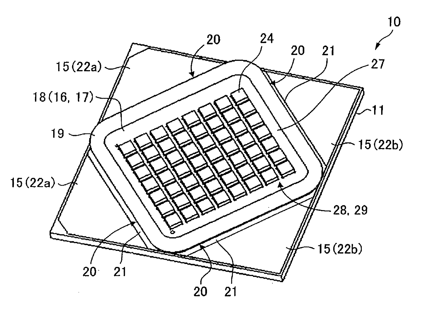
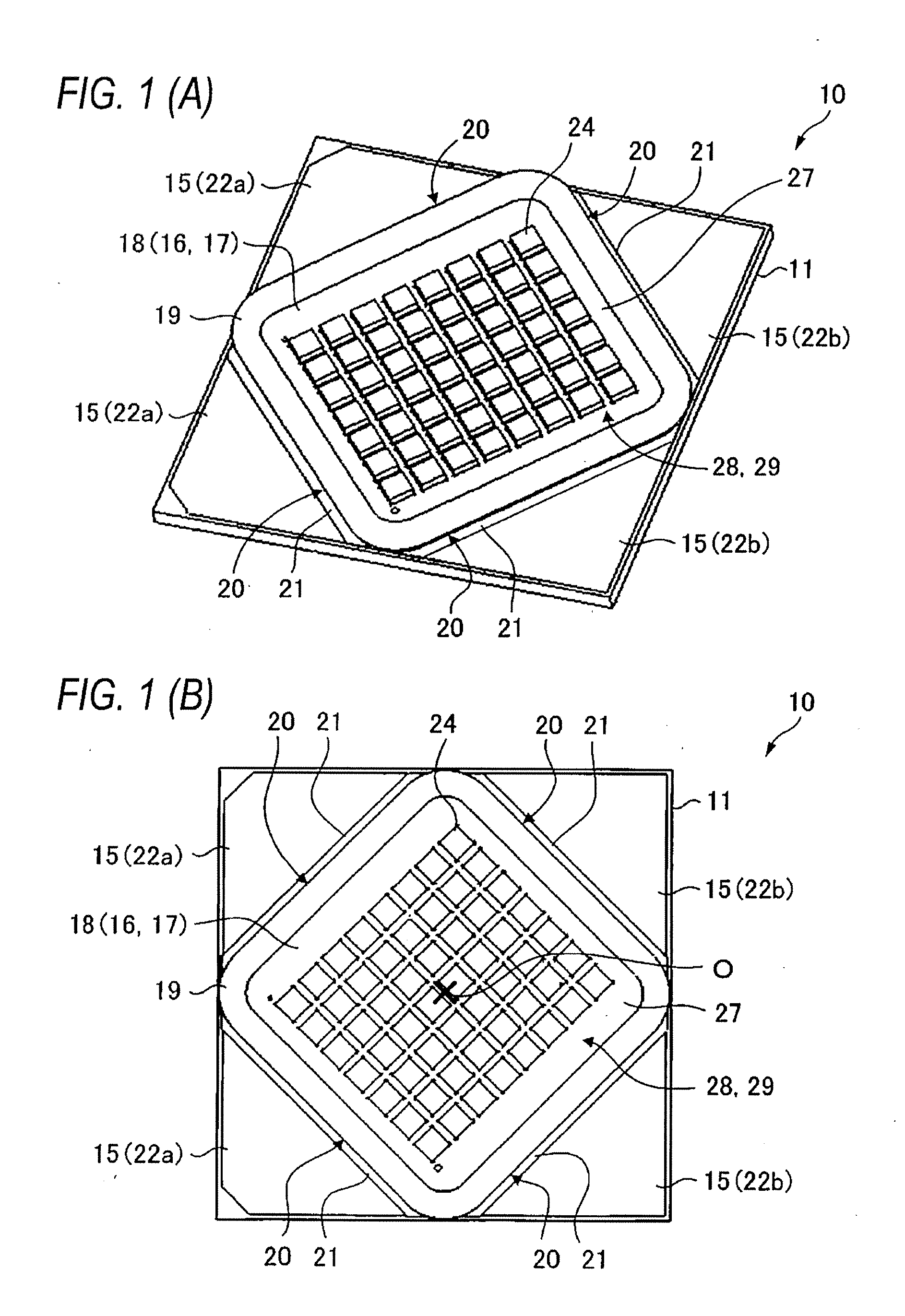
[0110]The following operation and advantages can be realized for the light emitting device 10 in Embodiment 1.

[0111][1] On the substrate 11, there is the wall portion 21 formed between the sealing frame 19 and the external electrodes 22a, 22b. Consequently, when the solder 23 is applied by soldering on the external electrodes 22a, 22b, as indicated by arrow a in FIG. 3, there is no way that solder 23 or solder flux (not shown in the drawing) can ride over the wall portion 21.

[0112]Consequently, it is possible to prevent corrosion of the light emitting portion 29 (sealing region 28) by the solder 23 or the solder flux. As a result, it is possible to prevent decrease in the luminance, generation of uneven light emission and degradation in the light emission quality caused by contamination of the light emitting portion 29.

[0113][2] Because there is the slit 20 formed between the wall portion 21 and the sealing frame 19, when the sealing member 27...

embodiment 2

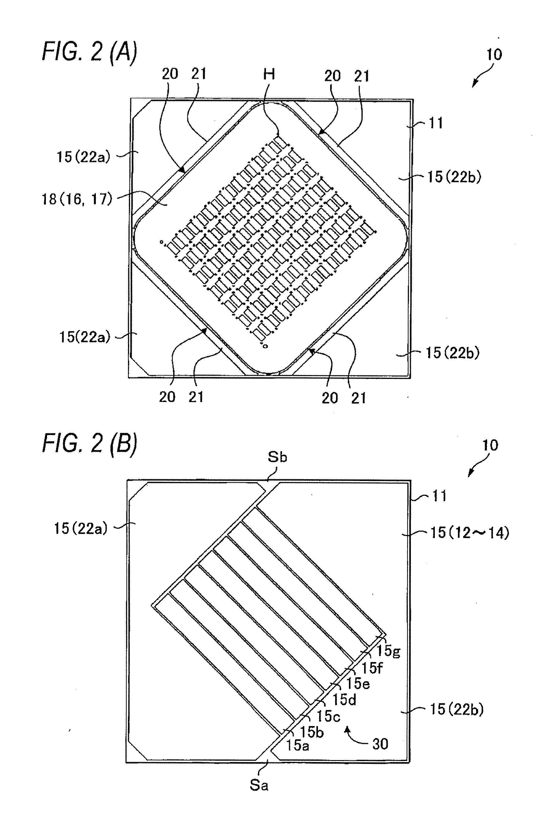
[0132]As shown in FIGS. 3 to 6, the light emitting device 100 of Embodiment 2 comprises a substrate 11, an adhesive layer 12, a heat dissipation layer 13, an adhesive layer 14, a wiring layer 15 (wiring regions 15a through 15g), an insulating layer 16, a reflective layer 17, a protective film 18, a sealing frame 19, a slit 20, a wall portion 21, external electrodes 22a, 22b, solder 23, LED chips 24, bumps 25, electrode pads 26, a sealing member 27, a sealing region 28, a light emitting portion 29, a wiring pattern 30, as well as opening portion H of the insulating layer 16, reflective layer 17 and protective film 18, gaps Sa, Sb of the wiring pattern 30, and a gap (slit) 101 of the insulating layer 16, reflective layer 17 and protective film 18.

[0133]Embodiment 2 differs from Embodiment 1 in the following features.

[0134][a] As shown in FIG. 5, the light emitting portion 29 has a flat round shape, and the substrate 11 and the light emitting portion 29 are superposed with each other w...

embodiment 3

[0142]As shown in FIG. 7, the light emitting device 200 of Embodiment 3 comprises a substrate 11, an adhesive layer 12, a heat dissipation layer 13, an adhesive layer 14, a wiring layer 15, an insulating layer 16, a reflective layer 17, a protective film 18, a sealing frame 19, a slit 20, a wall portion 21, external electrodes 22a, 22b, solder 23, LED chips 24, bumps 25, electrode pads 26, a sealing member 27, a sealing region 28, a light emitting portion 29, a wiring pattern 30, as well as opening portion H of the insulating layer 16, reflective layer 17 and protective film 18.

[0143]Embodiment 3 differs from Embodiment 1 in the following feature: the sealing frame 19 is formed on the wiring layer 15 in the outer side portion of the protective film 18, and, at the same time, it is formed in contact with the outer peripheral surface of the laminated film (insulating layer 16, reflective layer 17, protective film 18) along the outer edge of the protective film 18.

[0144]Consequently, a...


PUM


Abstract

There is a reflective layer covering almost the entire surface of the light emitting portion except the portions where the light emitting elements are arranged, it is possible to increase the reflectivity of the light emitting portion to realize a higher luminance. In addition, the heat generated from the light emitting elements can be dissipated through the reflective layer, so that it is possible to prevent overheat of the light emitting device, and it is thus possible to improve the reliability of the light emitting device.

Description

BACKGROUND OF THE INVENTION[0001]1. Field of the Invention[0002]The present invention relates to a light emitting device.[0003]2. Description of the Related Art[0004]Patent Reference 1 discloses a light emitting device, wherein a square-shaped flip chip of light emitting diodes and a square-shaped sub-mount are superposed with each other with their centers aligned with each other, and, at the same time, the flip chip is set rotated by 45° with respect to the sub-mount, and two lead-out electrodes are formed with respect to the flip chip on the upper surface exposed regions of the sub-mount.[0005]Patent Reference 2 discloses a light emitting device, wherein a plurality of linear shaped wiring patterns are arranged parallel with each other on an insulating substrate, and it has a light emitting portion, wherein a plurality of light emitting elements are carried between the wiring patterns while they are electrically connected to the wiring patterns; and the light emitting portion is s...

Claims


Application Information

Patent Timeline
IPC IPC(8): H01L27/15
CPCH01L25/0753H01L33/60H01L33/62H01L2224/16H01L2924/07811H01L2924/00
Inventor SHIMONISHI, SYOTATAJIMA, HIROYUKITSUCHIYA, YOSUKESENGOKU, AKIRA
Owner TOYODA GOSEI CO LTD
Why Eureka
Try Eureka