Non-volatile memory device and method of manufacturing the same

a non-volatile memory and memory device technology, applied in semiconductor devices, instruments, electrical devices, etc., can solve the problems of increasing the erase time, physical limitations, and reducing the size of the memory cell, so as to improve the erase speed of the non-volatile memory device

Active Publication Date: 2013-01-10
SK HYNIX INC
View PDF2 Cites 75 Cited by
  • Summary
  • Abstract
  • Description
  • Claims
  • Application Information

AI Technical Summary

Benefits of technology

[0008]An embodiment of this disclosure relates to a 3-D non-volatile memory device and a method of manufacturing the same, which are capable of improving the erase speed of the non-volatile memory device having generally U-shaped memory strings.

Problems solved by technology

A reduction in the size of the memory cells, however, is physically limited.
In this erase operation, however, there are disadvantages in that erase operation signals have complicated waveforms and the erase time is increased in order to induce the GIDL and the reliability of the select gate is deteriorated.

Method used


Image

  • Non-volatile memory device and method of manufacturing the same
  • Non-volatile memory device and method of manufacturing the same
  • Non-volatile memory device and method of manufacturing the same

Examples


first embodiment

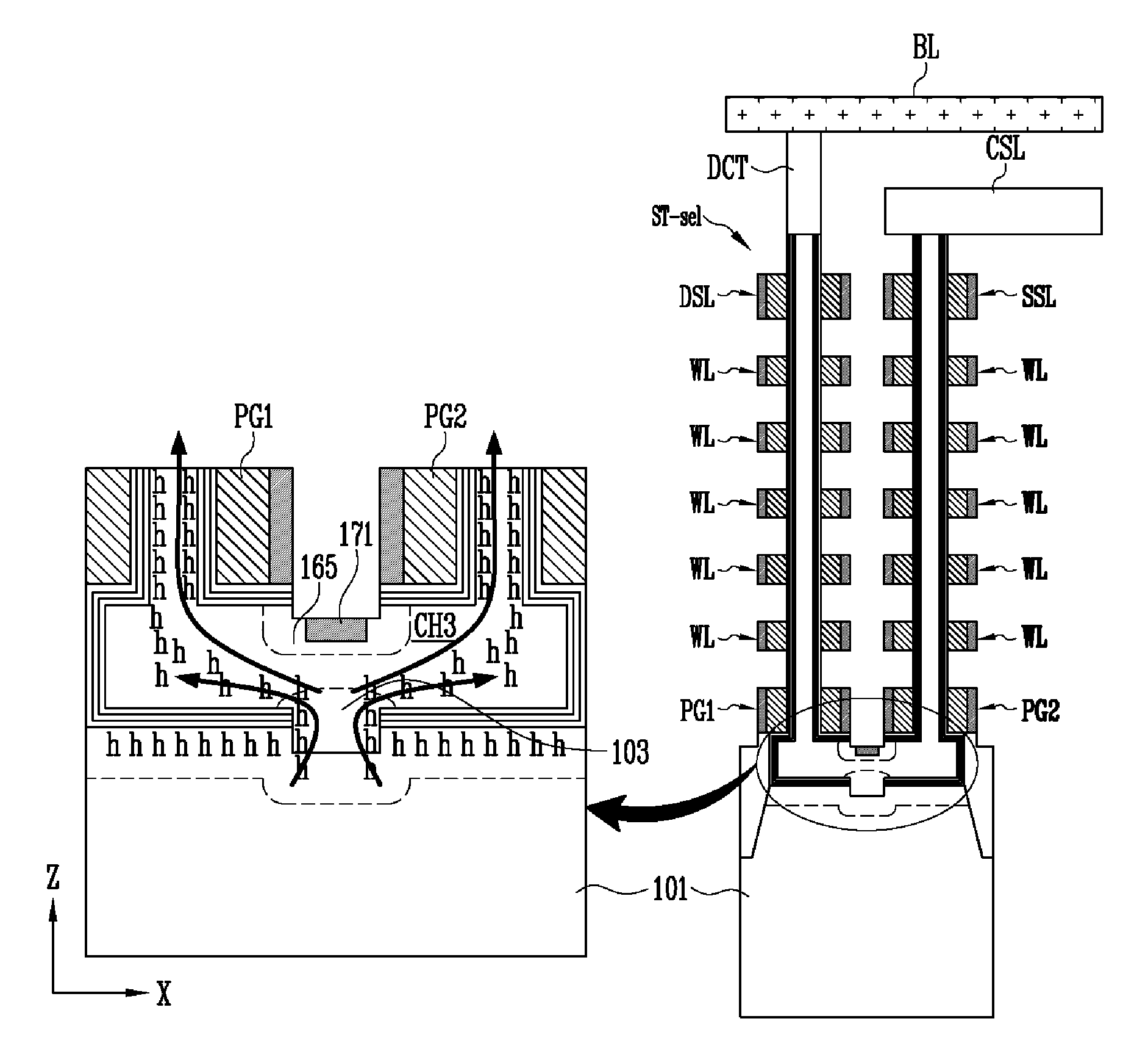
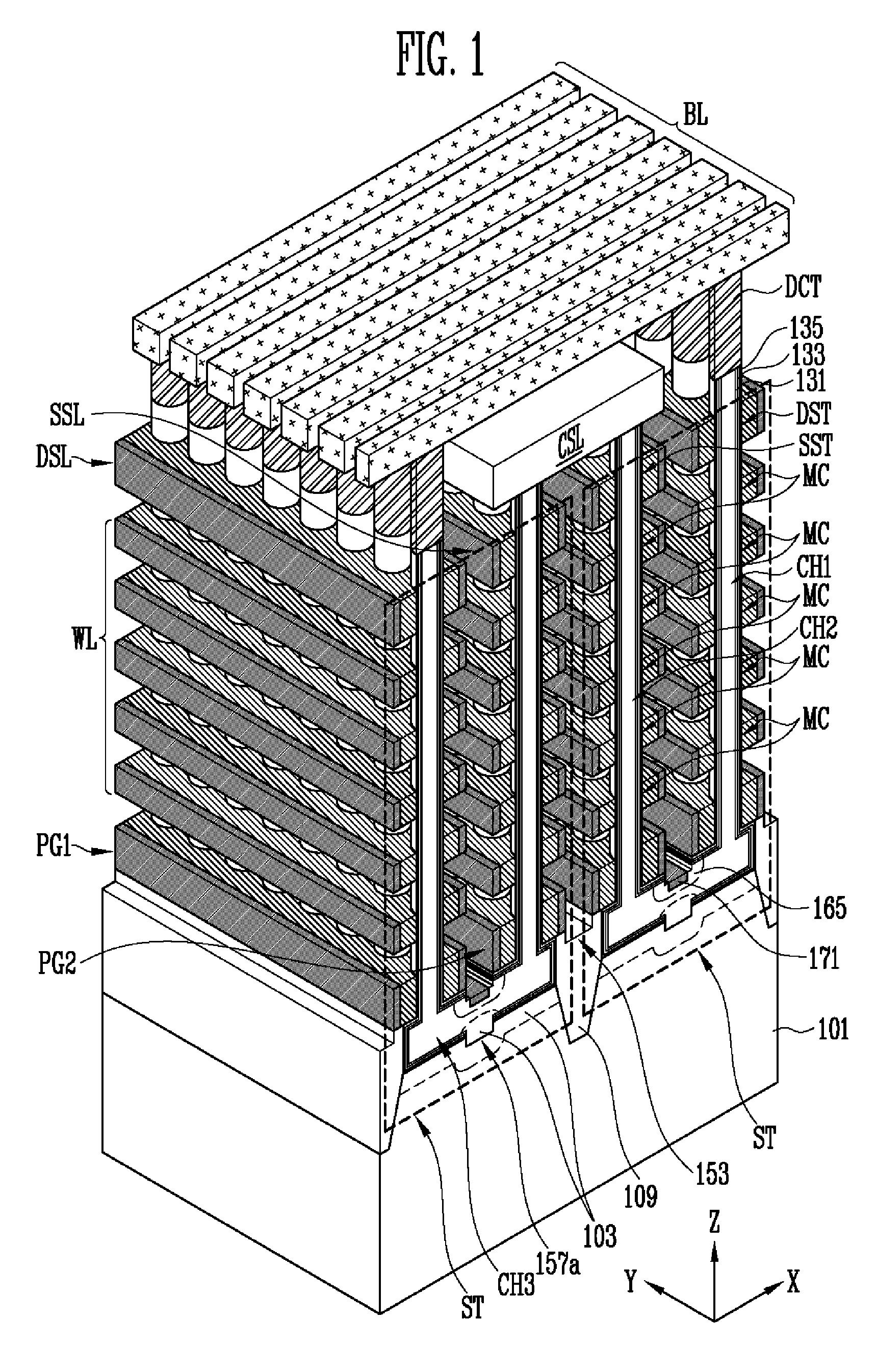
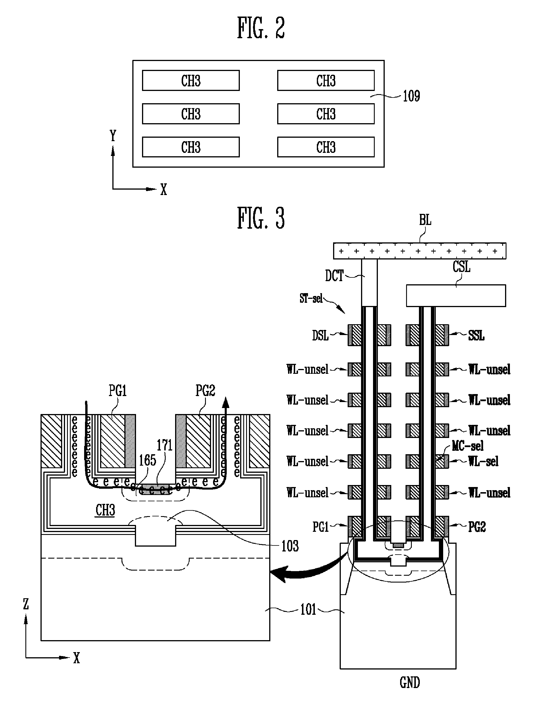
[0027]FIG. 1 is a diagram illustrating a non-volatile memory device according to this disclosure. It is to be noted that parts of insulating layers are not illustrated in FIG. 1, for the sake of convenience.

[0028]Referring to FIG. 1, the non-volatile memory device according to the first embodiment may include a plurality of memory strings ST arranged substantially in a matrix form including a plurality of columns and a plurality of rows. Each of the memory strings ST may include a channel layer coupled to a semiconductor substrate 101. The channel layer of the memory string ST may include a generally U-shaped channel layer and a channel layer extension unit 157a. The generally U-shaped channel layer may include first and second vertical channel layers CH1 and CH2 and a pipe channel layer CH3 formed to couple the first and the second vertical channel layers CH1 and CH2 together. The first and the second vertical channel layers CH1 and CH2 may upwardly protrude from the semiconductor ...

second embodiment

[0108]FIG. 8 is a diagram illustrating a non-volatile memory device according to this disclosure.

[0109]Referring to FIG. 8, the non-volatile memory device according to the second embodiment may include a plurality of memory string ST arranged substantially in a matrix form including a plurality of columns and a plurality of rows. Each of the memory strings ST may include a generally U-shaped channel layer and a channel layer extension part 357a generally extended from the generally U-shaped channel layer to the semiconductor substrate 301. The generally U-shaped channel layer may include first and second vertical channel layers CH1 and CH2 and a pipe channel layer CH3 formed to couple the first and the second vertical channel layers CH1 and CH2. The first and the second vertical channel layers CH1 and CH2 may upwardly protruded from the semiconductor substrate 301, formed generally in parallel in the Z direction, and spaced apart from each other. The pipe channel layer CH3 may be co...


PUM

PropertyMeasurementUnit
voltageaaaaaaaaaa
voltageaaaaaaaaaa
ground voltageaaaaaaaaaa

Abstract

A non-volatile memory device includes first and second vertical channel layers generally protruding upwardly from a semiconductor substrate substantially in parallel; a first gate group configured to include a plurality of memory cell gates which are stacked substantially along the first vertical channel layer and are isolated from each other with an interlayer insulating layer interposed substantially between the memory cell gates; a second gate group configured to include a plurality of memory cell gates which are stacked substantially along the second vertical channel layer and are isolated from each other with the interlayer insulating layer interposed substantially between the memory cell gates; a pipe channel layer configured to couple the first and the second vertical channel layers; and a channel layer extension part generally extended from the pipe channel layer to the semiconductor substrate and configured to couple the pipe channel layer and the semiconductor substrate.

Description

CROSS-REFERENCE TO RELATED APPLICATION[0001]The present application claim priority to Korean patent application number 10-2011-0066804 filed on Jul. 6, 2011, the entire disclosure of which is incorporated herein by reference in its entirety.BACKGROUND[0002]1. Technical Field[0003]Embodiments of this disclosure relate generally to a non-volatile memory device and a method of manufacturing the same and, more particularly, to a non-volatile memory device having a three-dimensional (3-D) structure and a method of manufacturing the same.[0004]2. Related Art[0005]As the memory device field, such as non-volatile memory devices, is advanced, there is an increasing demand for the high degree of integration of the memory devices. In a known art, the degree of integration of memory devices within a certain area is increased by using a method of reducing the size of memory cells which are arranged over a semiconductor substrate in a two-dimensional (2-D) manner. A reduction in the size of the m...

Claims


Application Information

Patent Timeline
Patent Type & Authority Applications(United States)
IPC IPC(8): H01L29/78H01L21/762
CPCH01L29/7926G11C16/0466H01L27/11582H10B43/27H01L21/823487H01L27/0688H01L21/76237H01L21/76294
Inventor YOO, HYUN SEUNG
Owner SK HYNIX INC
Why Eureka
Try Eureka