Erasing method and device for non-volatile memory

A technology of non-volatile memory and storage block, which is applied to the erasing of non-volatile memory devices and the field of erasing devices of non-volatile memory devices, which can solve the problems of slow speed, time-consuming and time-consuming, etc.

Active Publication Date: 2010-12-22
GIGADEVICE SEMICON (BEIJING) INC
View PDF10 Cites 14 Cited by
  • Summary
  • Abstract
  • Description
  • Claims
  • Application Information

AI Technical Summary

Problems solved by technology

Obviously, this serial erasing method is time-consuming
Furthermore, because actually a flash memory includes more memory blocks, the capacity of the flash memory is getting bigger and bigger, and in order to reduce the number of erasing and writing of the Flash, the prior art also tends to adopt smaller memory blocks to As an erasing unit, in this case, there will be more storage blocks in a flash memory. Using this method of erasing the entire Flash chip one by one in block units is not only time-consuming, but also slow. Erasing efficiency is relatively low

Method used


Image

  • Erasing method and device for non-volatile memory
  • Erasing method and device for non-volatile memory
  • Erasing method and device for non-volatile memory

Examples


Embodiment Construction

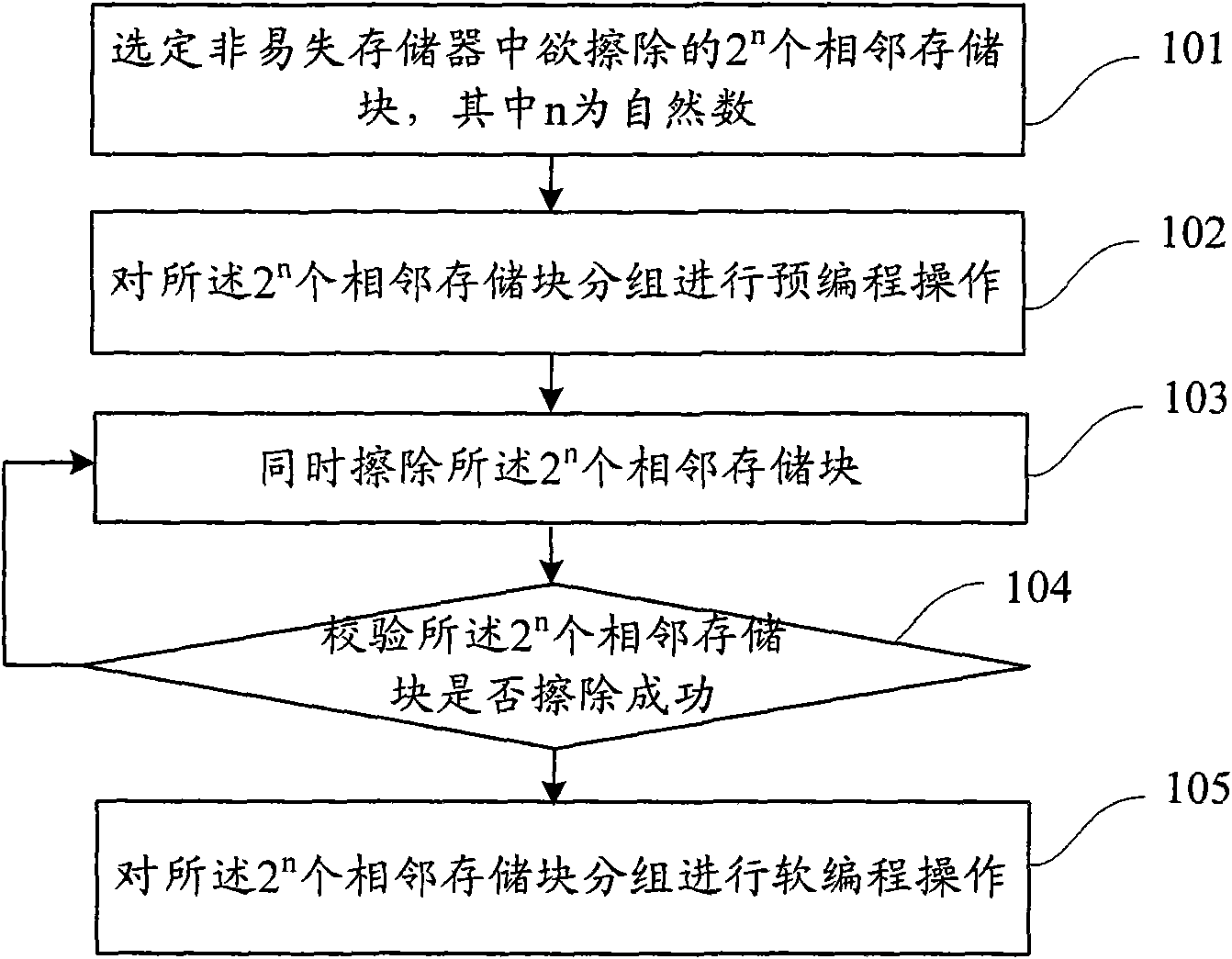
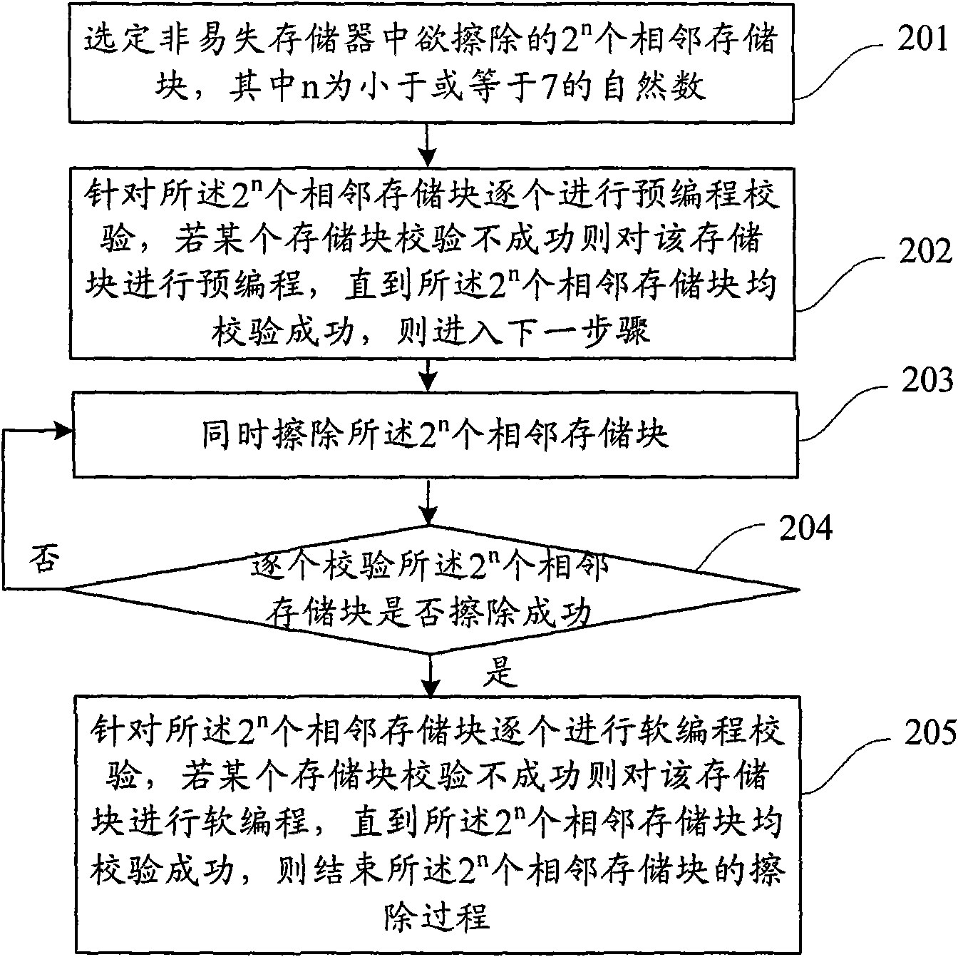
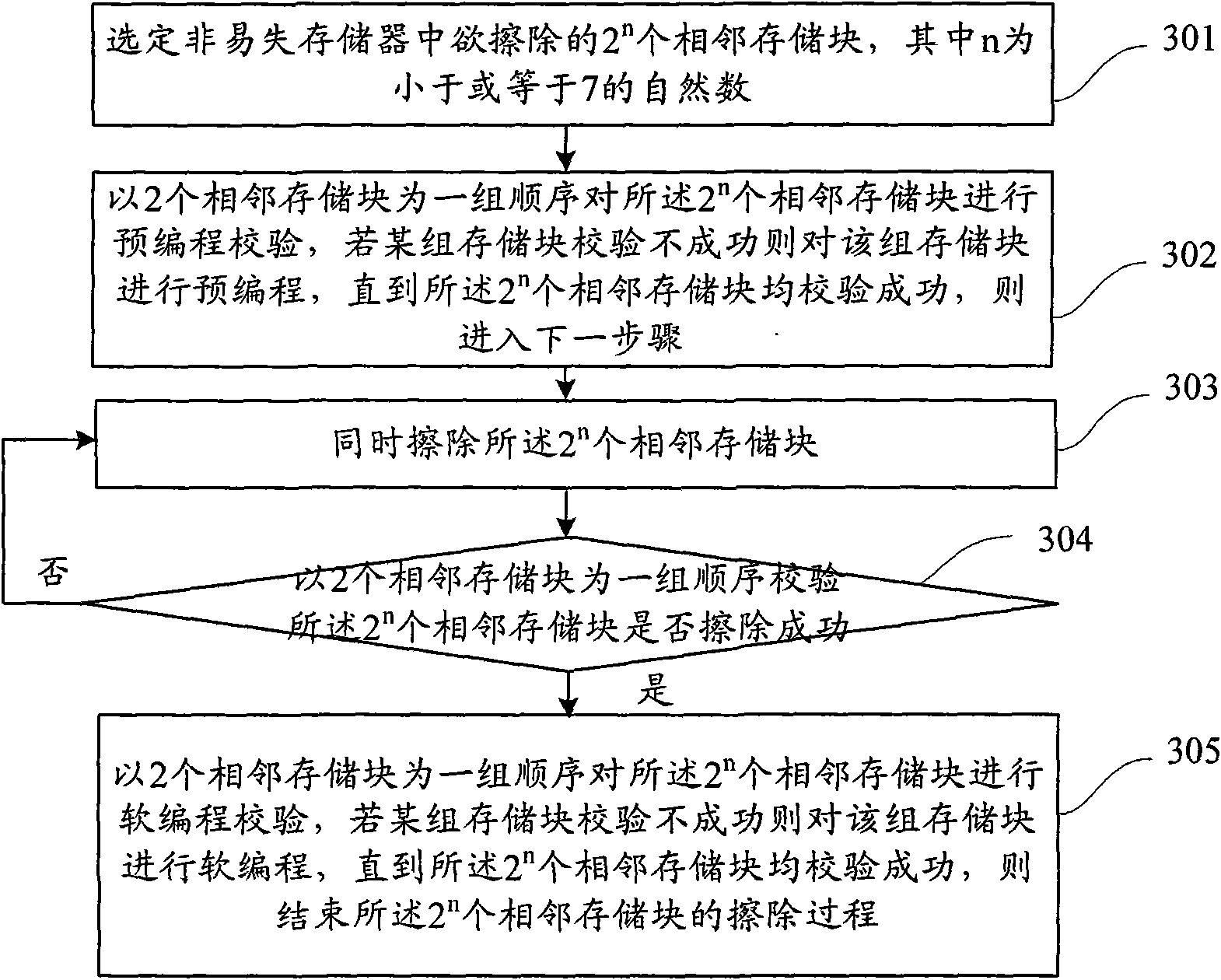
[0079] In order to make the above objects, features and advantages of the present invention more comprehensible, the present invention will be further described in detail below in conjunction with the accompanying drawings and specific embodiments.

[0080] In order for those skilled in the art to better understand the present invention, the following briefly introduces the basic principles of the non-volatile memory.

[0081] The non-volatile memory is composed of a storage unit (cell). The cell includes a capacitor and a transistor. The data in the cell depends on the charge stored in the capacitor, and the switch of the transistor controls the access of the data. Generally speaking, a cell may include a source (source, S), a drain (drain, D), a gate (gate, G), and a floating gate (floating gate, FG), and the FG may be connected to a voltage VG. If VG is a positive voltage, a tunnel effect occurs between FG and the drain D, so that electrons are injected into FG, causing the...


PUM


Abstract

The invention discloses an erasing method for a non-volatile memory. The method comprises the following steps of: selecting a target, namely, selecting 2n to-be-erased adjacent memory blocks in the non-volatile memory, wherein n is a natural number; performing pre-programming operation, namely, pre-programming the 2n adjacent memory blocks in groups; erasing, namely, simultaneously erasing the 2n adjacent memory blocks; checking the erasing, namely, checking whether the 2n adjacent memory blocks are successfully erased in groups, if so, performing soft programming operation, and otherwise, returning to the erasing step; and performing the soft programming operation, namely, performing the soft programming operation on the adjacent memory blocks in groups. The method can save erasing time and improve erasing speed and erasing efficiency.

Description

technical field [0001] The invention relates to the technical field of semiconductor memory, in particular to an erasing method for a nonvolatile memory device and an erasing device for a nonvolatile memory device. Background technique [0002] With the rapid development and wide application of various electronic devices and embedded systems, such as computers, personal digital assistants, mobile phones, digital cameras, etc., there is a great need for a device that can be programmed many times, has a large capacity, is fast to read and write, and can be erased. Convenient, simple, less peripheral devices, low-cost non-volatile (can still maintain the stored data information in the case of power failure) storage device. The non-volatile memory device emerges as the times require under this background demand. A non-volatile memory is usually also a MOS transistor, with a source (source), a drain (drain), a gate (gate), and a floating gate (floating gate). It can be seen tha...

Claims


Application Information

Patent Timeline
Patent Type & Authority Applications(China)
IPC IPC(8): G11C16/10
Inventor 舒清明潘荣华苏志强
Owner GIGADEVICE SEMICON (BEIJING) INC
Why Eureka
Try Eureka