Multi-level non-volatile memory

a non-volatile memory, multi-level technology, applied in the direction of digital storage, transistors, instruments, etc., can solve the problems of requiring a long time, and achieve the effect of improving the reliability of the devi

Active Publication Date: 2009-04-14
POWERCHIP SEMICON MFG CORP
View PDF5 Cites 15 Cited by
  • Summary
  • Abstract
  • Description
  • Claims
  • Application Information

AI Technical Summary

Benefits of technology

[0008]Accordingly, the present invention is directed to provide a multi-level non-volatile memory, a manufacturing method thereof, and an operation method thereof for improving the reliability of the device.
[0009]According to another aspect of the present invention, a multi-level non-volatile memory, a manufacturing method thereof, and an operation method thereof are provided for simplifying the processes and increasing the process window.
[0010]According to yet another aspect of the present invention, a multi-level non-volatile memory, a manufacturing method thereof, and an operation method thereof are provided for reducing the programming time and increasing the erasing speed of the memory cells.

Problems solved by technology

However, when a memory in the NOR non-volatile memory device is used as a multi-level memory cell, the threshold voltage for determining various data states has small distribution range, thus, in the programming operation of conventional NOR non-volatile memory, multiple programming steps and programming confirmation steps have to be executed to make the threshold voltage of the programmed memory cell to be within a predetermined distribution range, which may require a long time.

Method used


Image

  • Multi-level non-volatile memory
  • Multi-level non-volatile memory
  • Multi-level non-volatile memory

Examples


Embodiment Construction

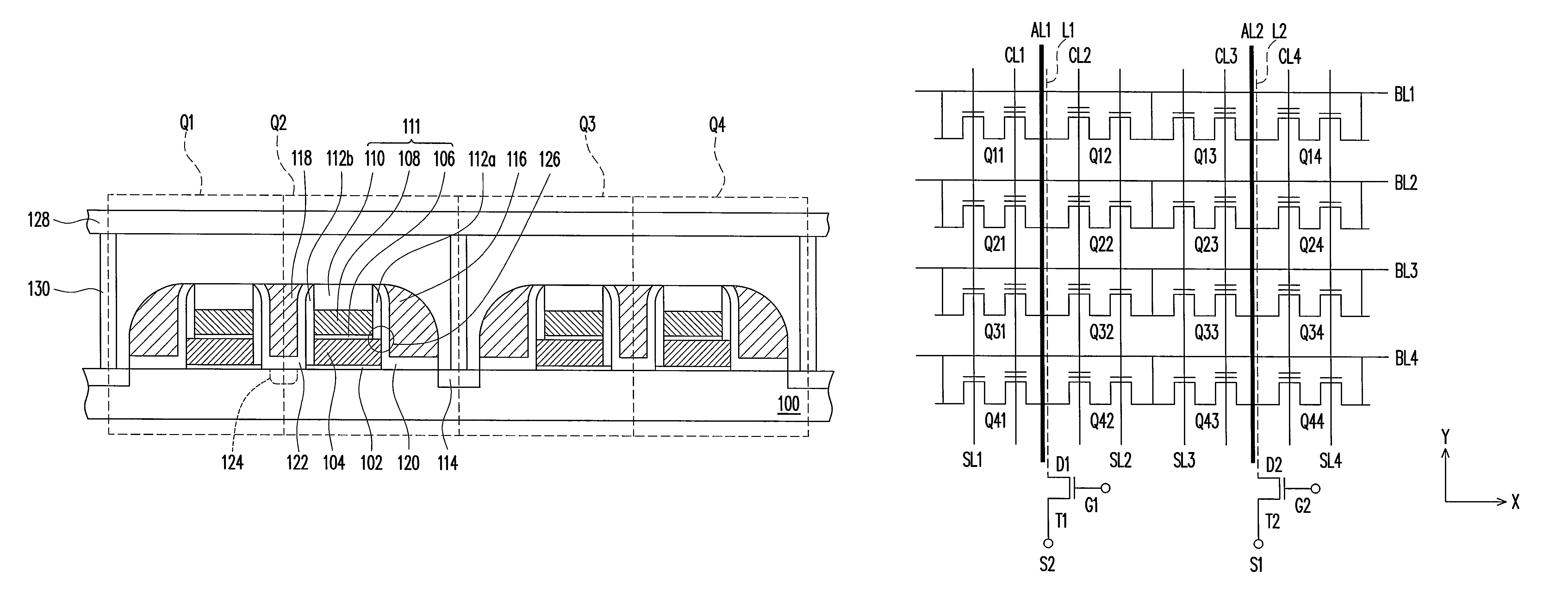
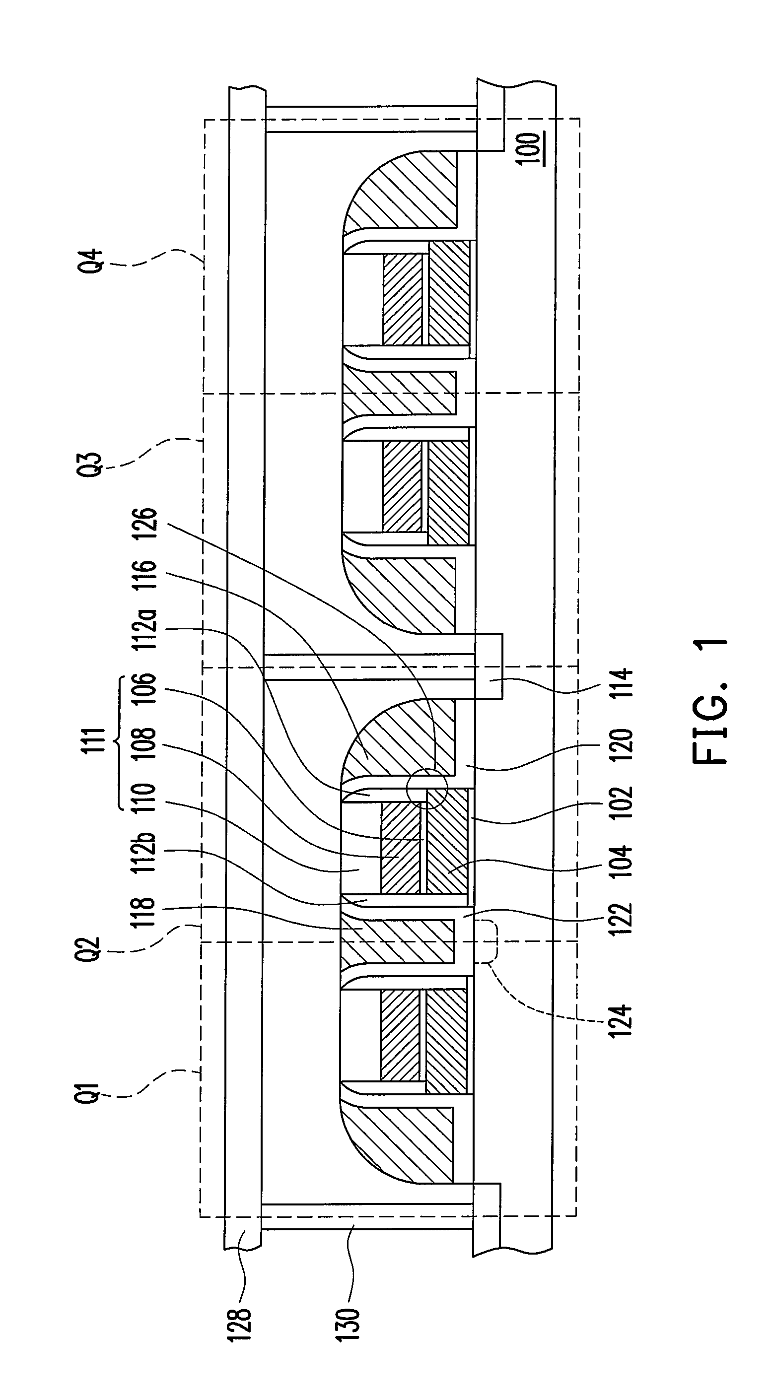
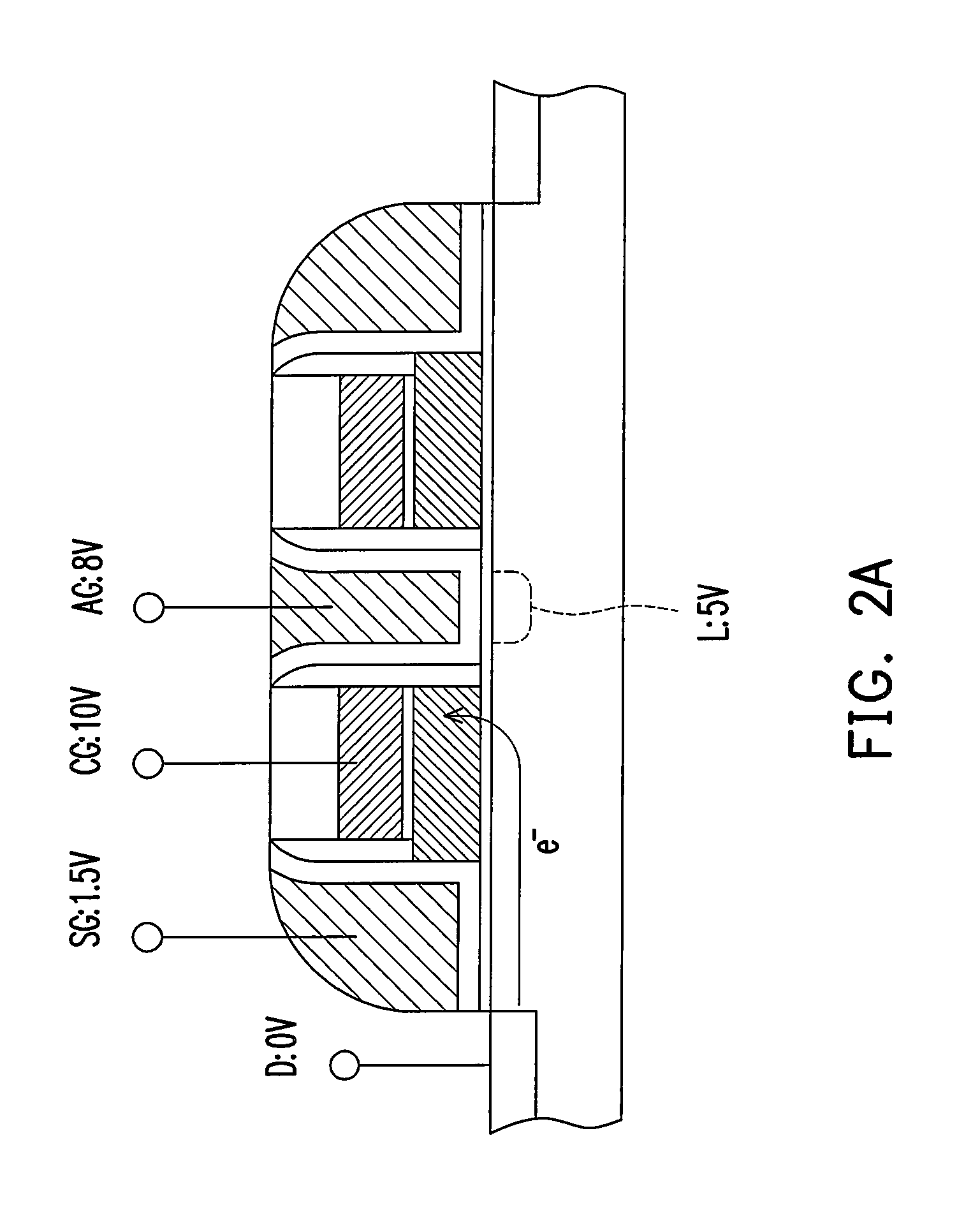
[0071]FIG. 1 is a cross-sectional view of a non-volatile memory according to an embodiment of the present invention.

[0072]Referring to FIG. 1, the multi-level non-volatile memory provided by the present invention includes, for example, a plurality of memory cells Q1, Q2, Q3, and Q4 disposed on the substrate 100. Each of the memory cells Q1, Q2, Q3, and Q4 includes a tunneling dielectric layer 102, a charge storage layer 104, an inter-gate dielectric layer 106, a control gate 108, a cap layer 110, spacers 112a, 112b, a doped region 114, a select gate 116, an assist gate 118, and dielectric layers 120, 122. The inter-gate dielectric layer 106, the control gate 108, and the cap layer 110 form a stacked layer 111.

[0073]The control gate 108 is, for example, disposed on the substrate 100. The material of the control gate 108 is, for example, doped polysilicon.

[0074]The charge storage layer 104 is, for example, disposed between the control gate 108 and the substrate 100. The material of th...


PUM


Abstract

A multi-level non-volatile memory including a memory cell disposed on a substrate is provided. The memory cell includes a control gate, a charge storage layer, a doped region, a select gate, and an assist gate. The control gate is disposed on the substrate. The charge storage layer is disposed between the control gate and the substrate. The doped region is disposed in the substrate at the first side of the control gate. The select gate is disposed on the sidewall of the first side of the control gate and on the substrate between the control gate and the doped region. The assist gate is disposed on the sidewall of the second side of the control gate. An inversion layer is formed in the substrate below the assist gate when a voltage is applied to the assist gate.

Description

BACKGROUND OF THE INVENTION[0001]1. Field of the Invention[0002]The present invention relates to a semiconductor device. More particularly, the present invention relates to a multi-level non-volatile memory, a manufacturing method thereof, and an operation method thereof.[0003]2. Description of Related Art[0004]Non-volatile memory device has been widely applied to personal computers and electronic apparatuses for the operations of data writing, reading, and erasing can be performed repeatedly to a non-volatile memory device and the data stored in a non-volatile memory device will not be lost even after power supply is turned off.[0005]The floating gate and control gate of a typical non-volatile memory device are fabricated with doped polysilicon. The control gate is disposed on the floating gate directly, the floating gate and the control gate are isolated by a dielectric layer, and the floating gate and the substrate are isolated by a tunneling oxide (the so-called stacked gate fla...

Claims


Application Information

Patent Timeline
Patent Type & Authority Patents(United States)
IPC IPC(8): G11C11/34
CPCG11C16/0433H01L21/28273H01L27/115H01L27/11521H01L29/42324H01L29/40114H10B69/00H10B41/30
Inventor HUNG, CHIH-WEICHOU, CHIH-CHEN
Owner POWERCHIP SEMICON MFG CORP
Why Eureka
Try Eureka