Method of fabricating algainp light-emitting diode and structure thereof

a technology of light-emitting diodes and algainp, which is applied in the direction of basic electric elements, electrical equipment, semiconductor devices, etc., can solve the problems of limited improvement of light output intensity, easy blocking of downward light emitted from flip-chip leds, etc., and achieves the reduction of total reflection, the effect of improving the light extraction efficiency of led devices and reducing the total reflection

Active Publication Date: 2005-12-29
EPISTAR CORP
View PDF1 Cites 74 Cited by
  • Summary
  • Abstract
  • Description
  • Claims
  • Application Information

AI Technical Summary

Benefits of technology

[0013] Additionally, a barrier layer is further placed between the metal reflective layer and the electrodes to prevent the electrodes from metal diffusing into the metal reflective layer and preserve the reflectivity of the metal reflective layer. The preferable material of the barrier layer is nickel (Ni), tungsten (W), titanium nitride (TiN), platinum (Pt), tungsten nitride (WN), zinc oxide (ZnO), or indium tin oxide (ITO).
[0014] Furthermore, the surface of the AlGaInP LED epitaxy is roughened to form a rough surface before bonding the transparent substrate material for reducing the total reflection phenomenon inside the LED device, and the light extraction efficiency of the LED device is improved. Even the transparent substrate material is roughened to reduce the total reflection for further improving the light output intensity of the LED device.
[0015] With the application of the present invention, the AlGaInP LED is finally supported by the transparent substrate material so that the light emitted from the AlGaInP LED is able to pass through the transparent substrate material and be successfully output outwards. Thus, the superiority of the flip chip LED structure is obtained for promoting the device reliability, and the light output intensity of the flip chip AlGaInP LED device is enhanced.
[0016] Further, the present invention utilizes the metal reflective layer placed between the AlGaInP LED epitaxy and the electrodes to reflect the light emitted downward from the LED structure, and the light emitted downward is thus reflected back into the LED and changed into a source of the light output upward. Therefore, the present invention makes use of the light emitted from the AlGaInP LED effectively for improving the light output intensity greatly, and the device brightness is increased.
[0017] Moreover, the surface of the AlGaInP LED structure or that of the transparent substrate material is further roughened in the present invention to increase the light extraction efficiency of the AlGaInP LED device and improve the light output intensity of the AlGaInP LED device.

Problems solved by technology

However, the light emitted upward from the flip chip AlGaInP LED is absorbed by the GaAs substrate and cannot pass through the GaAs for complete outward output.
Unfortunately, only the light emitted upward from the LED counts as light output; the light emitted downward is partially absorbed by the material below the LED device and is not another source for light output.
More particularly, the light emitted downward from the flip chip LED is easily blocked and scattered by electrodes.
Thus, the light output of the LED only depends on the diode luminance, and the light output intensity is limited in improvement.

Method used


Image

  • Method of fabricating algainp light-emitting diode and structure thereof
  • Method of fabricating algainp light-emitting diode and structure thereof
  • Method of fabricating algainp light-emitting diode and structure thereof

Examples


embodiment

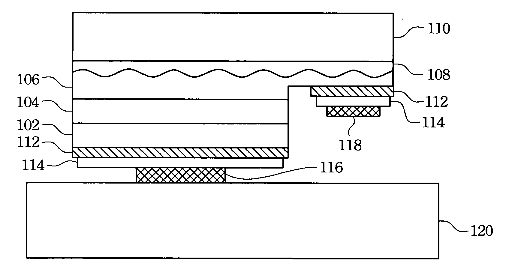
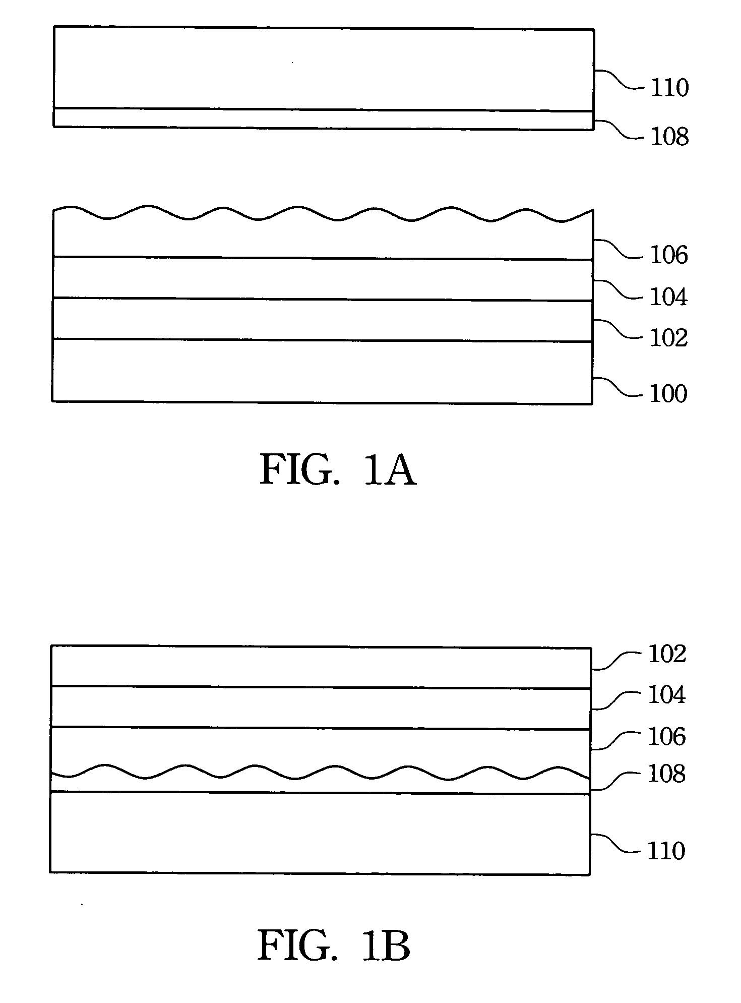
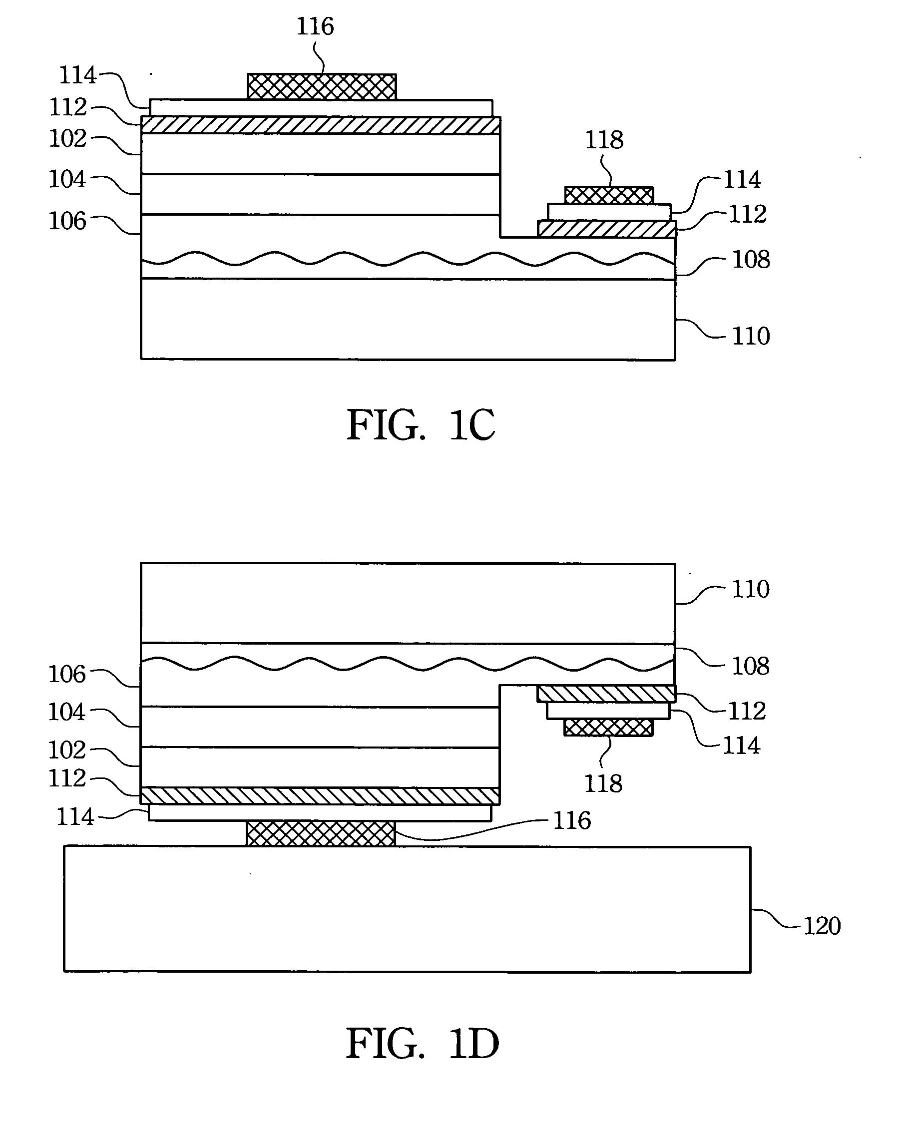
[0022] The present invention discloses a method of fabricating an AlGaInP LED and a structure therefore. FIGS. 1A-1D are cross-sectional, schematic diagrams showing the process for forming the AlGaInP LED in accordance with the preferred embodiment of the present invention.

[0023] In FIG. 1A, an AlGaInP LED epitaxy structure is first formed on a substrate 100, in which the substrate 100 is, for example, GaAs for obtaining a good crystallization quality of the AlGaInP epitaxy layers. The AlGaInP LED epitaxy structure is fabricated by forming an n-type AlGaInP layer 102, an AlGaInP active layer 104, and a p-type AlGaInP layer 106 in turn on the substrate 100. Further, the surface of the p-type AlGaInP layer 106 is next roughened to form a rough surface; for example, a photolithography and etching process is utilized to micro-etch the surface of the p-type AlGaInP layer 106 for producing surface roughness of the p-type AlGaInP layer 106.

[0024] The active layer 104 may be a homo-struct...


PUM

PropertyMeasurementUnit
soft transparentaaaaaaaaaa
transparentaaaaaaaaaa
roughnessaaaaaaaaaa

Abstract

A soft transparent adhesive layer is utilized to bond a transparent substrate material onto an AlGaInP light-emitting diode epitaxy on a GaAs substrate, and the GaAs substrate is next removed entirely. Then, a mesa etching process is performed to form a first top surface and a second top surface on the AlGaInP light-emitting diode epitaxy for respectively exposing an n-type layer and a p-type layer in the AlGaInP light-emitting diode epitaxy. Next, a metal reflective layer and a barrier layer are formed on the AlGaInP light-emitting diode epitaxy in turn, and electrodes are finally fabricated on the barrier layer.

Description

FIELD OF THE INVENTION [0001] The present invention relates to a method of fabricating an AlGaInP light-emitting diode and a structure thereof, and more particularly, to a method of fabricating an AlGaInP light-emitting diode with high light output intensity. BACKGROUND OF THE INVENTION [0002] Because of the low cost, simple structure, low power consumption and small size thereof, the light emitting diode (LED) is applied in display and illumination technologies. AlGaInP LED devices have already attracted considerable attention in red, yellow, orange, and green LED development. [0003] For general AlGaInP LED fabrication, an AlGaInP LED device is formed on a GaAs substrate directly, while a cathode electrode and an anode electrode are respectively fabricated on different sides of the substrate. This conventional structure has a better current spreading efficiency, but an increased device package area is necessary. Therefore, a flip chip AlGaInP LED device has been gradually developed...

Claims


Application Information

Patent Timeline
Patent Type & Authority Applications(United States)
IPC IPC(8): H01L21/00H01L33/00
CPCH01L33/0079H01L33/0066H01L33/0093
Inventor LIAO, TIEN-FUCHANG, CHIH-SUNGCHEN, TZER-PERNG
Owner EPISTAR CORP
Why Eureka
Try Eureka