Production method of LED

A technology of light-emitting diodes and manufacturing methods, which is applied in the direction of electrical components, circuits, semiconductor devices, etc., can solve the problems of light output intensity limitation of light-emitting diodes, reduction of light output intensity of light-emitting diodes, and inability to be effectively used, so as to improve quality and The effect of brightness presentation, improvement of light extraction efficiency, and enhancement of light output intensity

Active Publication Date: 2010-09-29
EPISTAR CORP
View PDF5 Cites 2 Cited by
  • Summary
  • Abstract
  • Description
  • Claims
  • Application Information

AI Technical Summary

Problems solved by technology

[0009] However, due to the light emission of the flip-chip LED, when it is output upward, it will be absorbed by the upper substrate, and cannot penetrate the substrate, and then output to the outside of the LED.
Therefore, although the flip-chip LED has the advantages of packaging, it actually leads to a decrease in the light output intensity of the flip-chip LED.
[0010] In addition, because the improvement of the brightness of the LED is always the main development trend of the LED technology at present, but generally except for the part where the LED emits light directly upward, the light emitted from other directions will be partially absorbed by the material below the LED. It cannot be effectively used as a source of light output, especially the light emitting diode of the flip-chip type. The part emitted to the bottom of the light emitting diode is very easy to be blocked by electrodes or scattered.
Therefore, the light output intensity of the light-emitting diode mainly depends on the light-emitting characteristics of the light-emitting diode itself, so that the improvement of the light output intensity of the light-emitting diode is limited.

Method used


Image

  • Production method of LED
  • Production method of LED
  • Production method of LED

Examples


Embodiment 1

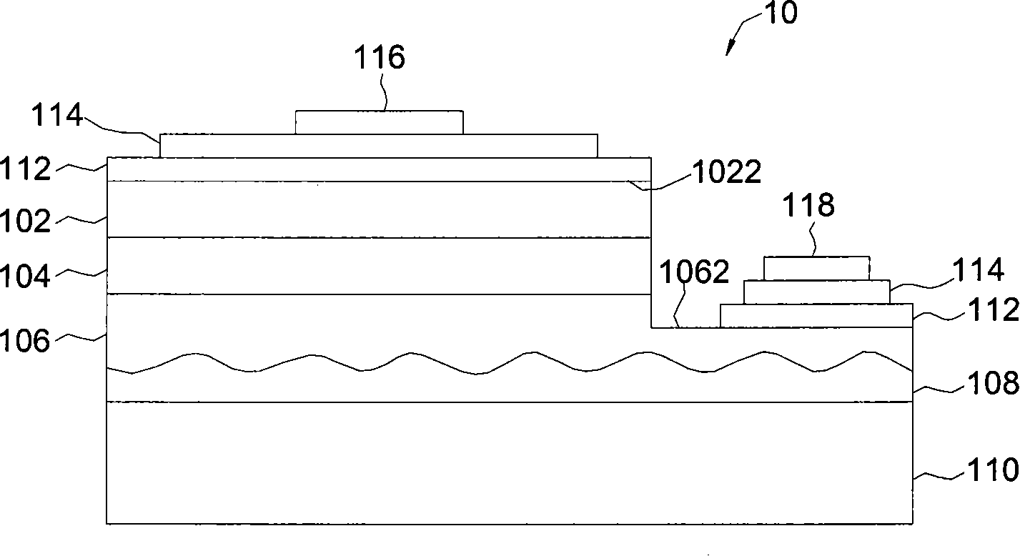
[0027] A flip-chip light emitting diode disclosed in the present invention, Figure 1A to Figure 1D It is a schematic cross-sectional view of a process flow of a flip-chip manufacturing method of a light emitting diode according to an embodiment of the present invention.

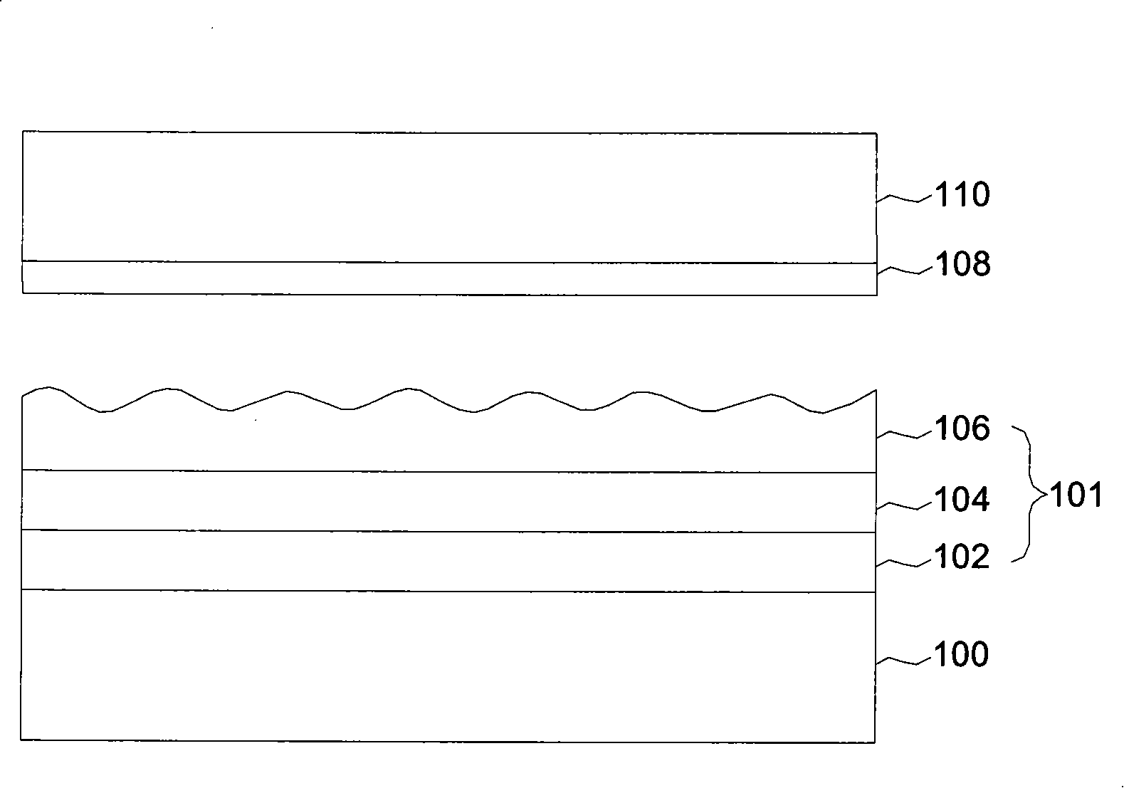
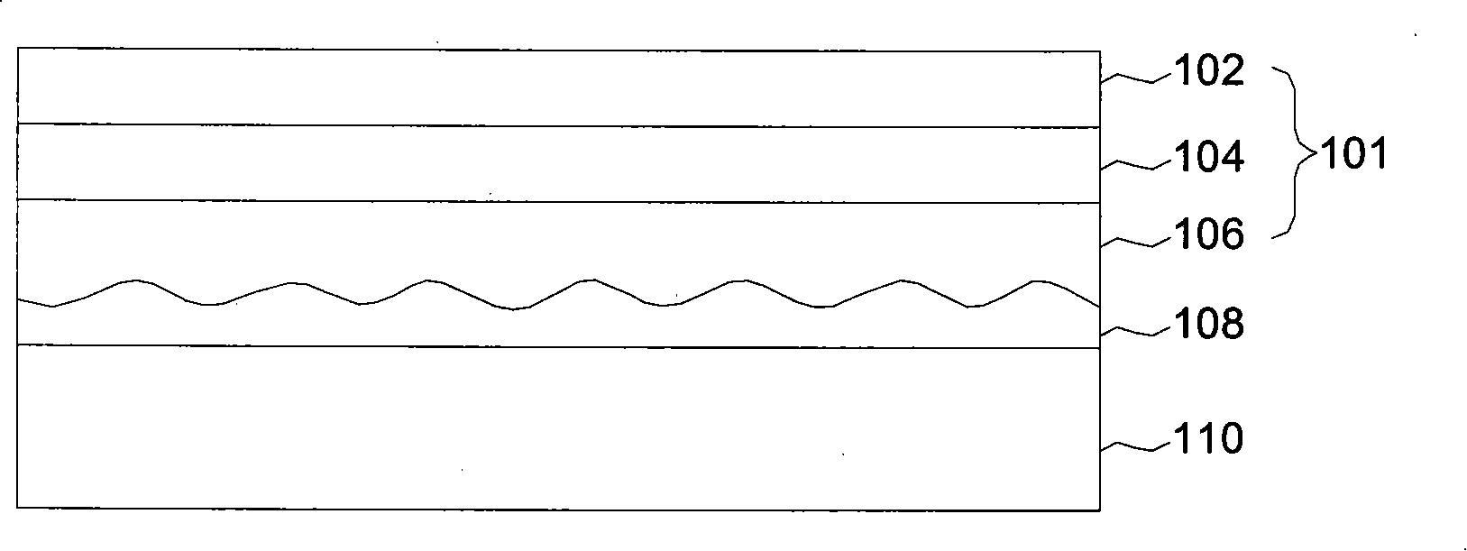
[0028] in Figure 1A In the first step, a light-emitting diode epitaxial structure 101 is fabricated on a substrate 100. The light-emitting diode epitaxial structure 101 described here includes aluminum gallium indium phosphide light-emitting diodes (AlGaInP) and aluminum gallium indium nitride light-emitting diodes (AlGaInN). In order to obtain an epitaxial structure with good crystal quality, when manufacturing aluminum gallium indium phosphide (AlGaInP) light-emitting diodes, the substrate 100 is selected from germanium (Ge), gallium arsenide (GaAs) or indium phosphorus (InP), and When manufacturing aluminum gallium indium nitride (AlGaInN) light-emitting diodes, the substrate 100 is selected from sapphire (S...

Embodiment 2

[0038] Reference figure 2 Shown is a schematic diagram of another flip-chip light emitting diode 20 according to a preferred embodiment of the present invention. In this embodiment, in addition to the steps described in embodiment 1, the upper surface of the transparent substrate 210 can be further roughened to form uneven surface characteristics, so that the light-emitting diodes can emit light outward. The increase further contributes to improving the light extraction efficiency of the light emitting diode and the light output intensity of the entire light emitting diode.

[0039] Furthermore, at the interface between the transparent substrate 210 and the soft transparent adhesive layer 208, and the lower surface of the transparent substrate 210, an uneven joint surface is formed, so that it has a rough surface characteristic of unevenness.

[0040] The roughening treatment of the upper and lower surfaces of the transparent substrate 210, for example, can be formed before the tr...

Embodiment 3

[0042] The present invention further discloses a flip-chip light emitting diode, such as Figure 3D As shown, Figure 3A-3D It is a schematic cross-sectional view of the flow of the flip-chip manufacturing method of the light emitting diode according to the preferred embodiment of the present invention.

[0043] According to the steps described in embodiment 1, an n-type semiconductor layer 302, a light-emitting active layer 304, and a p-type semiconductor layer 306 are respectively formed on the substrate 300 to fabricate a light-emitting diode epitaxial structure 301, such as Figure 3A Shown. Similarly, the light-emitting active layer 304 may have a homogenous structure, a single heterostructure, a double heterostructure, or a multiple quantum well structure.

[0044] Then, a temporary substrate 310 coated with a soft transparent adhesive layer 308 on the surface is attached to the light emitting diode epitaxial structure 301, and the temporary substrate 310 is attached using the...


PUM


Abstract

The invention provides a manufacturing method for an LED, which uses a soft and transparent bonding layer to joint a transparent parent metal with an epitaxial structure of the LED that is fabricated at the parent metal, and then removes the parent metal for transferring the epitaxial structure of the LED onto the transparent parent metal; afterwards the epitaxial structure of the LED is processed by mesa etching to lead the epitaxial structure of the LED to form a first upper surface and a second upper surface and simultaneously reveal an n-type semiconductor layer and a p-type semiconductorlayer, and then a metal reflecting layer and a barrier layer are formed at the epitaxial structure of the LED; and at last the electrodes are fabricated at the barrier layer.

Description

[0001] This application is a divisional application of the following applications, [0002] Application date of the original application: March 1, 2005, [0003] The application number of the original application: 2005100529590, [0004] The title of the invention of the original application: flip-chip light-emitting diode and its manufacturing method. Technical field [0005] The invention relates to a method for manufacturing a light emitting diode, and in particular to a method for manufacturing a flip-chip light emitting diode that can increase the light output intensity. Background technique [0006] Light Emitting Diode (LED) has the advantages of low production cost, simple structure, low power consumption, small size and easy installation, and is widely used in lighting source and display technology. [0007] Generally, traditional light-emitting diodes directly fabricate the epitaxial structure of the light-emitting diode on the substrate, and fabricate the cathode electrode an...

Claims


Application Information

Patent Timeline
Patent Type & Authority Patents(China)
IPC IPC(8): H01L33/00
Inventor 蔡宗良张智松陈泽澎
Owner EPISTAR CORP
Why Eureka
Try Eureka