

Diffusion layer for semiconductor devices
a technology of semiconductor devices and diffusion layers, applied in the field of metal oxidesemiconductor field-effect transistors, can solve the problems of short-channel characteristics degrading devices, hydrogen degrading negative bias temperature instability,
- Summary
- Abstract
- Description
- Claims
- Application Information
AI Technical Summary
Benefits of technology
Problems solved by technology
Method used
Image

Examples
Embodiment Construction
[0012] The making and using of the presently preferred embodiments are discussed in detail below. It should be appreciated, however, that the present invention provides many applicable inventive concepts that can be embodied in a wide variety of specific contexts. The specific embodiments discussed are merely illustrative of specific ways to make and use the invention, and do not limit the scope of the invention.
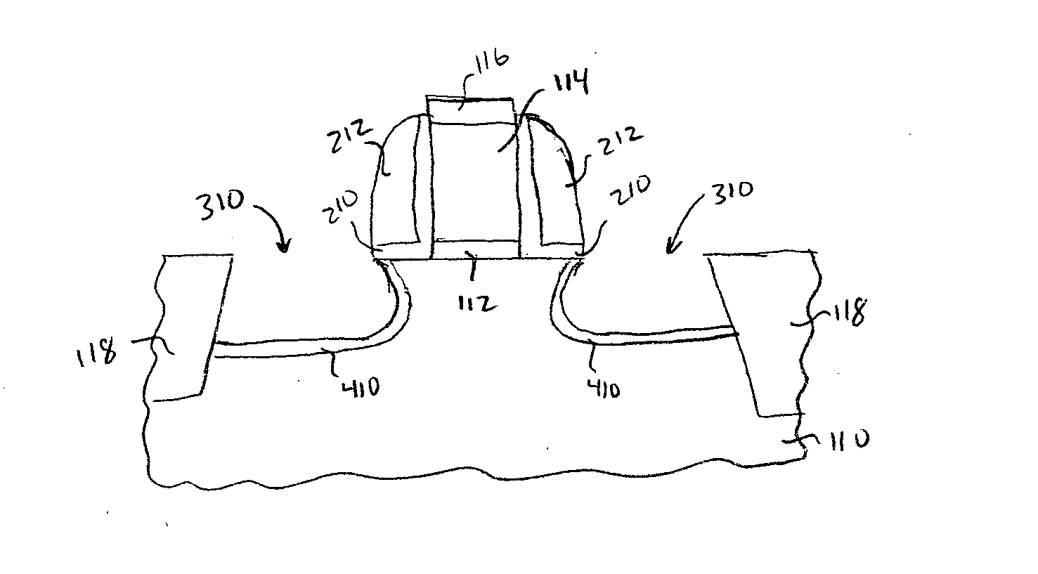
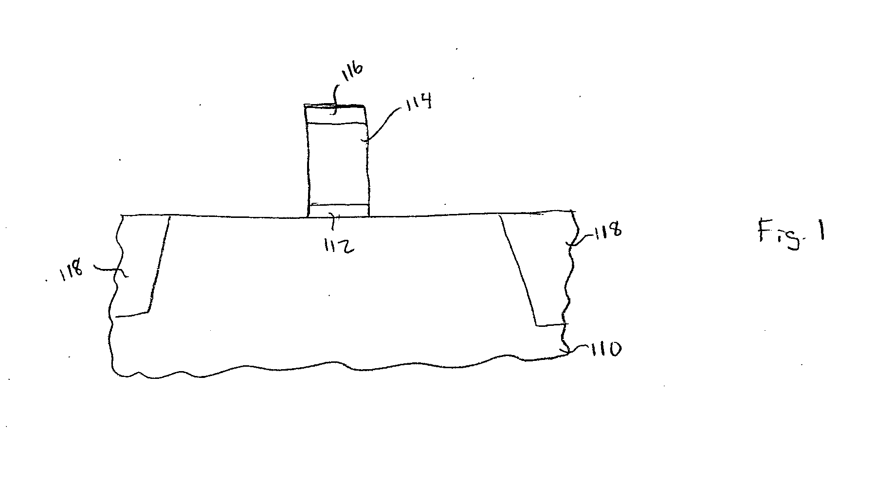
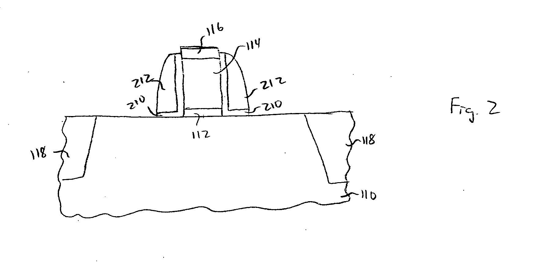
[0013]FIGS. 1-6 illustrate a method embodiment for fabricating a semiconductor device having a diffusion layer in accordance with an embodiment of the present invention. Embodiments of the present invention illustrated herein may be used in a variety of circuits. In particular, embodiments of the present invention are particularly useful for sub-65 nm transistor designs in which dopant penetration into the substrate may be particularly troublesome. This diffusion layer can improve the device reliability.
[0014] Referring first to FIG. 1, a substrate 110 is shown having a ga...
PUM
| Property | Measurement | Unit |
|---|---|---|
| width | aaaaa | aaaaa |
| depth | aaaaa | aaaaa |
| width | aaaaa | aaaaa |
Abstract
Description
Claims
Application Information